

Semiconductor package, electronic apparatus and method of manufacturing the semiconductor package
- Summary
- Abstract
- Description
- Claims
- Application Information
AI Technical Summary
Benefits of technology
Problems solved by technology
Method used
Image

Examples
Embodiment Construction
[0031]Reference will now be made to example embodiments, which are illustrated in the accompanying drawings, wherein like reference numerals may refer to like components throughout.
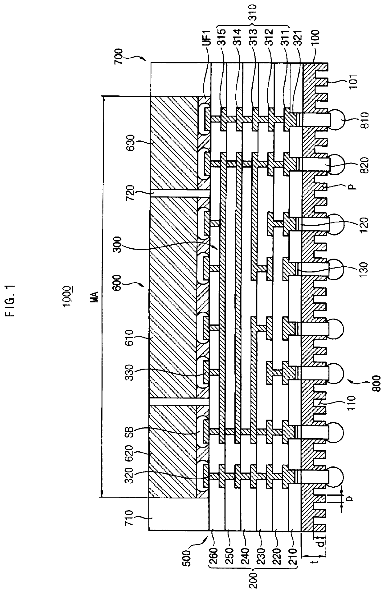
[0032]FIG. 1 is a cross-sectional view illustrating a semiconductor package in accordance with an example embodiment of the present disclosure.
[0033]Referring to FIG. 1, a semiconductor package 1000 in accordance with an example embodiment of the present disclosure may include an interposer 500 having a plurality of wiring structures 300 and a separation layer 100, a plurality of semiconductor devices 600 arranged on the interposer 500 side by side, a securing mold 700 securing the semiconductor devices 600 to the interposer 500 and a plurality of contact terminals 800 on a rear surface of the interposer 500. In the present example embodiment, a fan-out package is provided as the semiconductor package 1000 in which the semiconductor devices 600 are connected to the contact terminals 800 via the interposer...
PUM
 Abstract
Description
Claims
Application Information