Multi-spot scanning device, system and method

Active Publication Date: 2021-08-05
VISITECH INT LTD
View PDF1 Cites 0 Cited by
  • Summary
  • Abstract
  • Description
  • Claims
  • Application Information

AI Technical Summary

Benefits of technology

[0006]In accordance with a first aspect of the invention there is provided a confocal microscope device for scanning a two-dimensional array of illumination beams over a target surface and scanning a corresponding two-dimensional array of emission beams stimulated by the array of illumination beams on to a sensor of an imaging device. The device comprises first scanning optics operable to scan the array of illumination beams over the target surface along a first axis and scan the array of emission beams over the sensor along the first axis. The device further compris

Problems solved by technology

However, when imaging real-world samples, particularly living samples, illumination and emission PSFs are subject to diffraction which gives rise to interference between the PSFs.
In certain instances, this interference manifests as “striping” artefacts at the image plane and thus in the final ima

Method used


Image

  • Multi-spot scanning device, system and method
  • Multi-spot scanning device, system and method
  • Multi-spot scanning device, system and method

Examples


Embodiment Construction

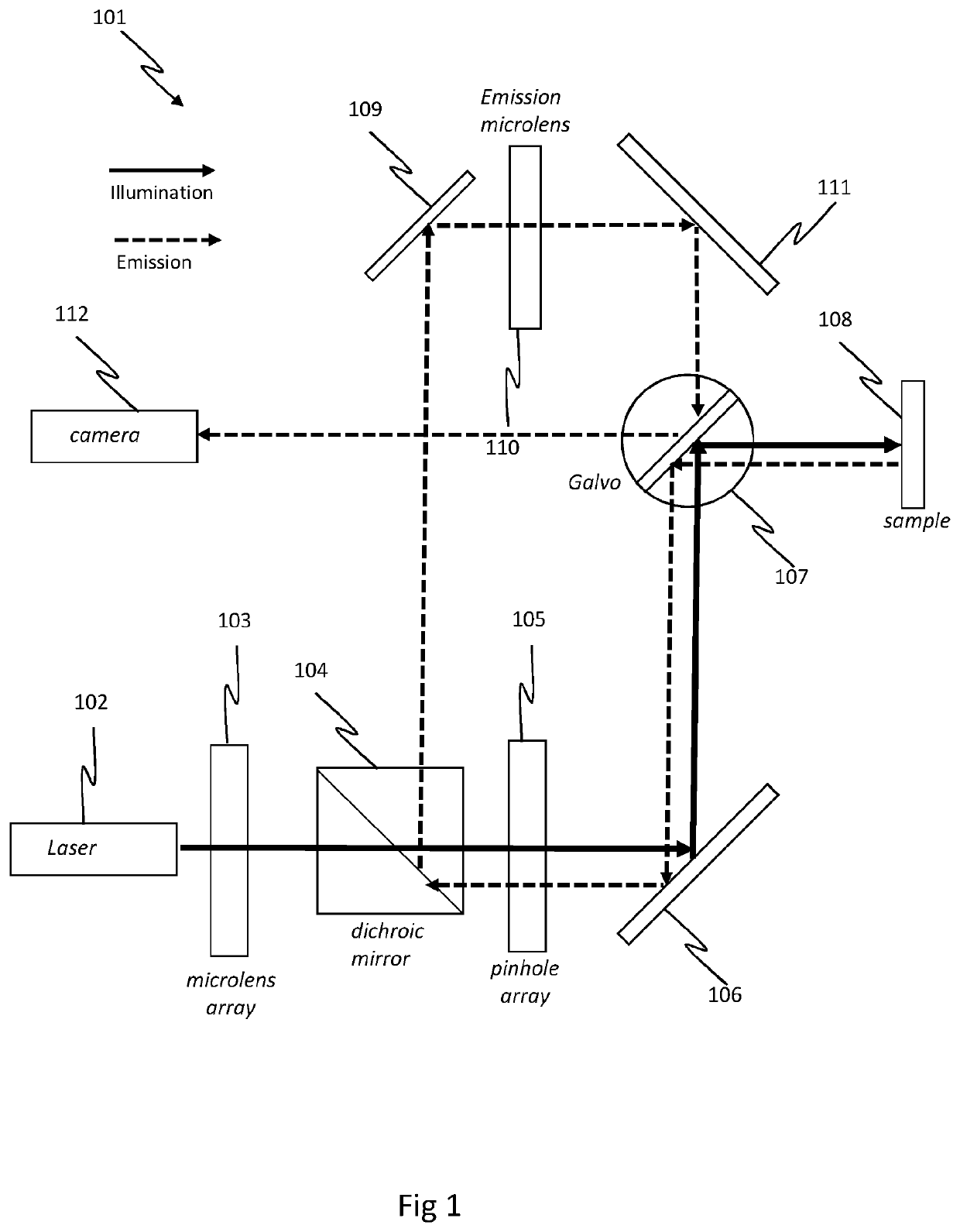
[0038]FIG. 1 provides a simplified schematic diagram of a conventional confocal scanning system 101.

[0039]The system comprises a laser light source 102, a two-dimensional microlens array 103, a dichroic mirror 104, a two-dimensional confocal pinhole array 105, a first mirror 106, a galvanometer mirror 107 and a sample stage on which is mounted a sample 108 (target surface). The system further comprises a second mirror 109, an emission microlens 110, a third mirror 111 and an imaging camera 112. As will be understood, a typical confocal scanning system will comprise further components, such as relay optics, however, for clarity such components are omitted from FIG. 1.

[0040]The system shown in FIG. 1 is sometimes referred to as a “super-resolution” imaging system by virtue of the provision of the emission microlens 110 (described in more detail below). Certain systems are provided without the emission microlens 110, but the operating principle is the same.

[0041]In use, collimated lase...


PUM


Abstract

A confocal microscope device for scanning a two-dimensional array of illumination beams over a target surface and scanning a corresponding two-dimensional array of emission beams stimulated by the array of illumination beams on to a sensor of an imaging device. The device comprises first scanning optics operable to scan the array of illumination beams over the target surface along a first axis and scan the array of emission beams over the sensor along the first axis. The device further comprises second scanning optics operable to deflect, on a second axis, the array of illumination beams as they are scanned over the target surface along the first axis, such that uneven stimulation of the target surface by the array of illumination beams due to interference of the illumination beams is reduced, and deflect, on the second axis, the array of emission beams as they are scanned over the sensor of the imaging device along the first axis such that uneven stimulation of the sensor by the array of emission beams due to interference of the emission beams is reduced.

Description

TECHNICAL FIELD[0001]The present invention relates to an improved confocal scanning, device, system and method.BACKGROUND[0002]Confocal imaging systems are well known and widely used. Advanced multi-point confocal scanning systems use a technique in which an array of illumination beams is scanned across a sample plane usually by virtue of a galvanometer mirror, piezo mirror or spinning “Nipkow” disk. A corresponding array of emission beams are stimulated (typically through fluorescence) from the sample which are passed through a pinhole array with the same architecture as the illumination beams. This removes any out of focus light so that when the emission beams are scanned or relayed onto a sensor of an imaging device, a focussed image is produced.[0003]Such systems enable very high temporal and spatial resolution to be achieved. Each illumination beam incident on the sample surface and corresponding emission beam incident on the imaging plane can be modelled as a point spread func...

Claims


Application Information

Patent Timeline
IPC IPC(8): G02B26/08G02B21/00G02B27/58
CPCG02B26/0875G02B21/0032G02B27/58G02B21/0044G02B21/0048G02B21/0036G02B21/0072G02B21/0076G02B21/0024
Inventor COLEMAN, STEVENROBERTS, ANDREWSHEBLEE, JAFER
Owner VISITECH INT LTD
Why Eureka
Try Eureka