Substrate with multilayer reflective film, reflective mask blank, reflective mask, and method for producing semiconductor device

Active Publication Date: 2021-08-12
HOYA CORP
View PDF0 Cites 0 Cited by
  • Summary
  • Abstract
  • Description
  • Claims
  • Application Information

AI Technical Summary

Benefits of technology

The present disclosure is about a reflective mask used in semiconductor device manufacturing. The mask has a multilayer reflective film with high reflectance and low film stress. The film's reflectance is maintained even if there is mixing of the layers during heat treatment after formation. This disclosure provides a method for manufacturing a semiconductor device using the reflective mask. The technical effects are improved exposure and reduced film stress during semiconductor device manufacturing.

Problems solved by technology

If mixing proceeds excessively, the problem occurs in which reflectance of the multilayer reflective film with respect to exposure light decreases.

Method used


Image

  • Substrate with multilayer reflective film, reflective mask blank, reflective mask, and method for producing semiconductor device
  • Substrate with multilayer reflective film, reflective mask blank, reflective mask, and method for producing semiconductor device
  • Substrate with multilayer reflective film, reflective mask blank, reflective mask, and method for producing semiconductor device

Examples


example 1

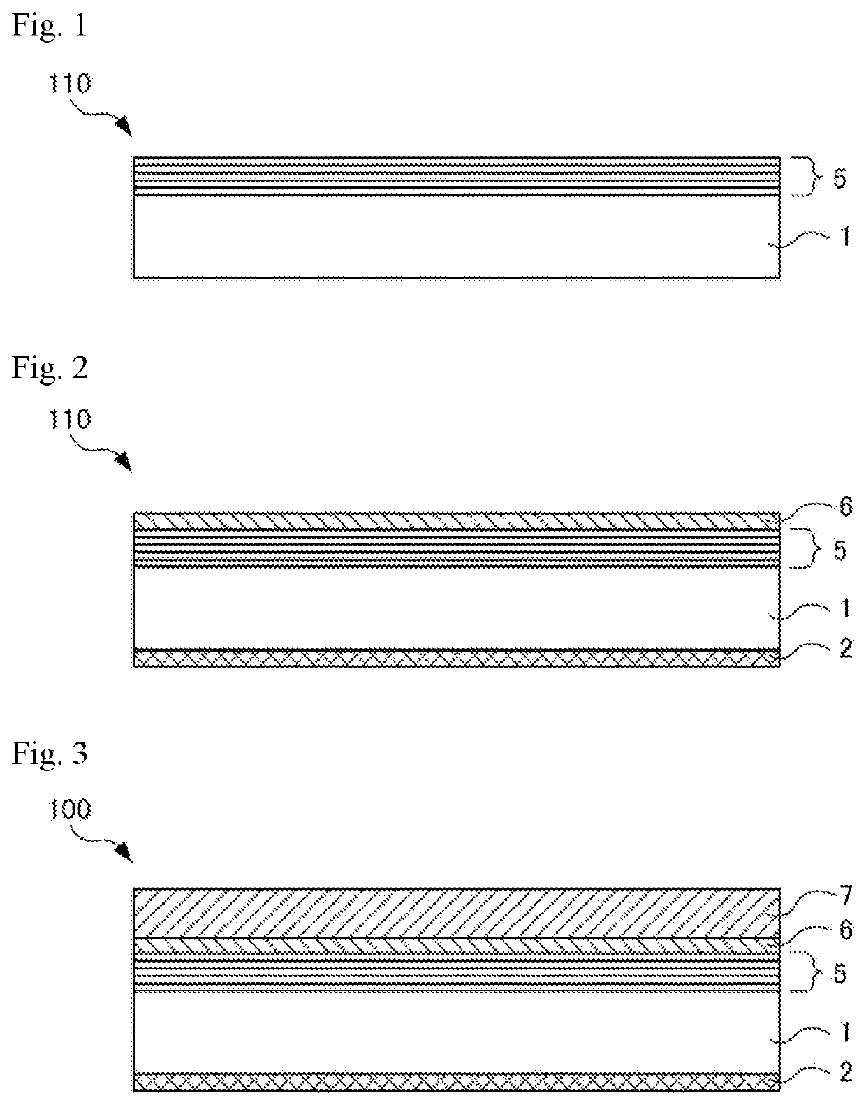
[0129]The substrate with multilayer reflective film 110 having the multilayer reflective film 5 formed on one main surface of the substrate 1 was fabricated for Example 1, as shown in FIG. 1. Fabrication of the substrate with multilayer reflective film 110 of Example 1 was carried out in the manner indicated below.

[0130]((Substrate 1))

[0131]A low thermal expansion glass substrate in the form of a 6025 size SiO2—TiO2-based glass substrate measuring about 152 mm×152 mm×6.35 mm, in which both the first main surface and second main surface were polished, was prepared as the substrate 1. Polishing consisting of a coarse polishing step, precision polishing step, local processing step and touch polishing step was carried out so as to obtain a flat and smooth main surface.

[0132]((Multilayer Reflective Film 5))

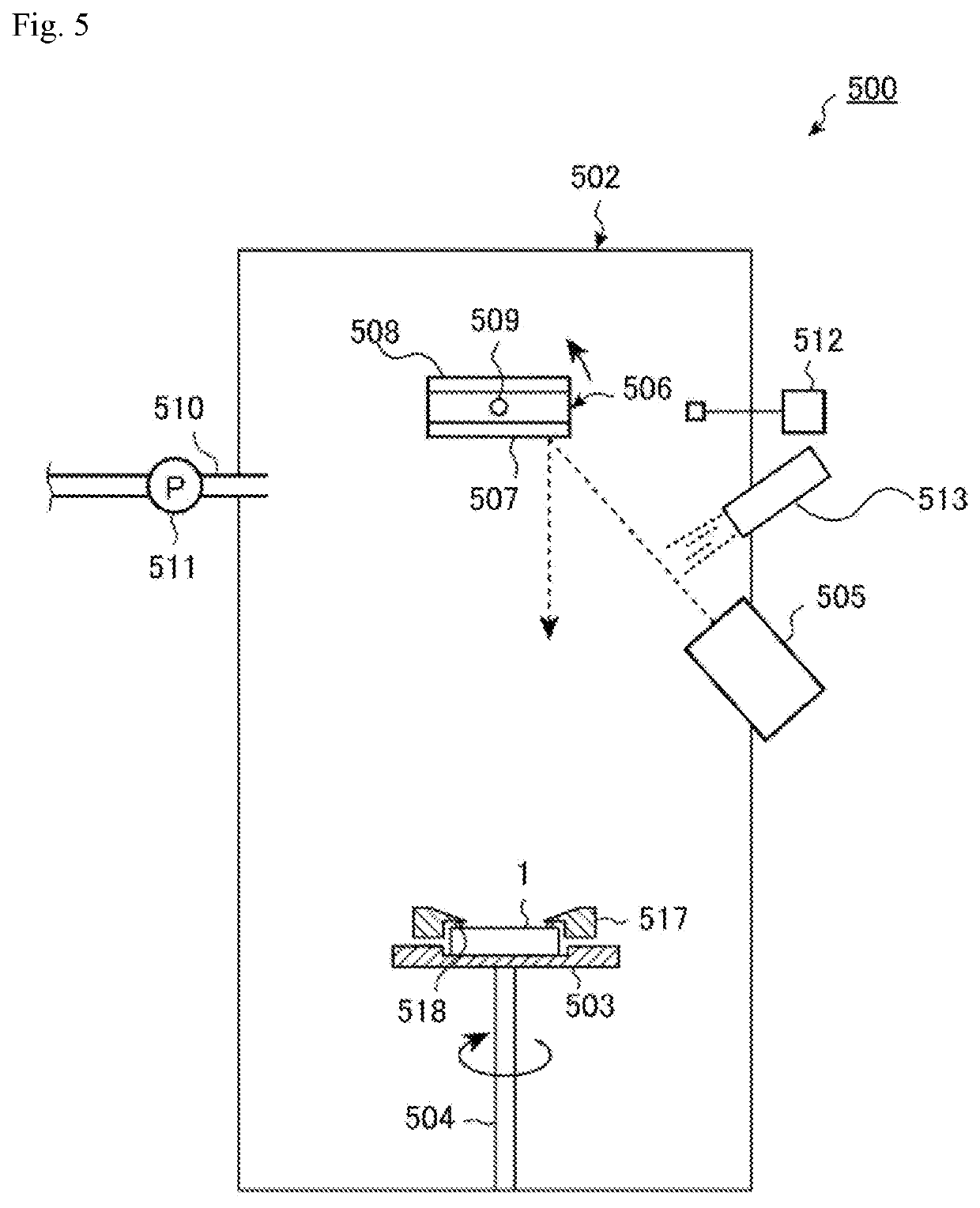
[0133]The multilayer reflective film 5 was formed on the first main surface of the aforementioned substrate 1 using the ion beam sputtering apparatus 500 shown in FIG. 5. This multilay...

example 2

[0140]The substrate with multilayer reflective film 110 having the multilayer reflective film 5 formed on the first main surface of the substrate 1 was manufactured in the same manner as Example 1 for Example 2 as shown in Table 1.

[0141]The substrate with multilayer reflective film 110 of Example 2 was annealed in the same manner as Example 1 with the exception of changing the annealing temperature to 200° C. In addition, reflectance and degree of flatness of the multilayer reflective film 5 were measured before and after annealing. The results of those measurements are shown in Table 1.

example 3

[0142]The substrate with multilayer reflective film 110 having the multilayer reflective film 5 formed on the first main surface of the substrate 1 was manufactured in the same manner as Example 1 for Example 3 as shown in Table 1.

[0143]The substrate with multilayer reflective film 110 of Example 3 was annealed in the same manner as Example 1 with the exception of changing the annealing temperature to 260° C. In addition, reflectance and degree of flatness of the multilayer reflective film 5 were measured before and after annealing. The results of those measurements are shown in Table 1.


PUM

PropertyMeasurementUnit
Thicknessaaaaaaaaaa
Contentaaaaaaaaaa
Refractive indexaaaaaaaaaa

Abstract

Provided is a substrate with multilayer reflective film used to manufacture a reflective mask having a multilayer reflective film having high reflectance with respect to exposure light and little film stress. The substrate with multilayer reflective film is provided with a multilayer reflective film for reflecting exposure light, the substrate with multilayer reflective film comprising a multilayer film obtained by building up an alternating stack of low refractive index layers and high refractive index layers on a substrate, and the multilayer reflective film contains krypton (Kr).

Description

CROSS REFERENCE TO RELATED APPLICATIONS[0001]This application is a National Stage of International Application No. PCT / JP2018 / 022756 filed Jun. 14, 2018, which claims priority to Japanese Patent Application No. 2017-121485 filed Jun. 21, 2017, and the contents of which is incorporated by reference in its entirety.TECHNICAL FIELD[0002]The present disclosure relates to a reflective mask used to manufacture a semiconductor device and a substrate with multilayer reflective film and reflective mask blank used to manufacture a reflective mask. In addition, the present disclosure relates to a method of manufacturing a semiconductor device using the aforementioned reflective mask.BACKGROUND ART[0003]Accompanying the increasingly higher levels of integration of semiconductor devices in the semiconductor industry in recent years, there is a need for fine patterns that exceed the transfer limitations of conventional photolithography methods using ultraviolet light. Extreme ultraviolet (EUV) li...

Claims


Application Information

Patent Timeline
IPC IPC(8): G03F1/24H01L21/033G03F1/58
CPCG03F1/24G03F1/58H01L21/0332H01L21/0337C23C14/14G02B5/08G03F1/52G03F1/54G03F7/20
Inventor KOZAKAI, HIROFUMIONOUE, TAKAHIRO
Owner HOYA CORP
Why Eureka
Try Eureka