Method for Manufacturing Target Material for Copper Lead of TFT-LCD Array Substrate and Target Material

a technology of thin film transistors and target materials, applied in the field of sputtering targets, can solve the problems of easy control of orientation, disadvantageous improvement of tft-lcd array substrate quality, and difficult selection of crystalline plane orientation, etc., and achieves low electrical resistivity, small film stress, and low surface roughness

Inactive Publication Date: 2013-12-05
SHENZHEN CHINA STAR OPTOELECTRONICS TECH CO LTD
View PDF1 Cites 0 Cited by
  • Summary
  • Abstract
  • Description
  • Claims
  • Application Information

AI Technical Summary

Benefits of technology

[0009]An object of the present invention is to provide a method for manufacturing target material for a copper lead of a TFT-LCD array substrate, whereby a copper film made with a target material manufactured with the method is relatively low electrical resistivity, relatively small film stress, and relatively low surface roughness, and the process is simple and efficiency is high.

Problems solved by technology

Such a process cannot easily control orientation of grain in the steps of shaping through hot rolling / hot extrusion and annealing to recover crystallization so that it is hard to select the orientation of the crystalline plane (111) in making a Cu film.
Referring to FIG. 4, which is a picture showing surface roughness of a copper film manufactured by sputtering copper target material that is manufactured with a regular process, the surface roughness is Ra=2.73 nm, which is relatively high and is thus disadvantageous for improving quality of a TFT-LCD array substrate.

Method used


Image

  • Method for Manufacturing Target Material for Copper Lead of TFT-LCD Array Substrate and Target Material
  • Method for Manufacturing Target Material for Copper Lead of TFT-LCD Array Substrate and Target Material
  • Method for Manufacturing Target Material for Copper Lead of TFT-LCD Array Substrate and Target Material

Examples


Embodiment Construction

[0034]To further expound the technical solution adopted in the present invention and the advantages thereof, a detailed description is given to a preferred embodiment of the present invention and the attached drawings.

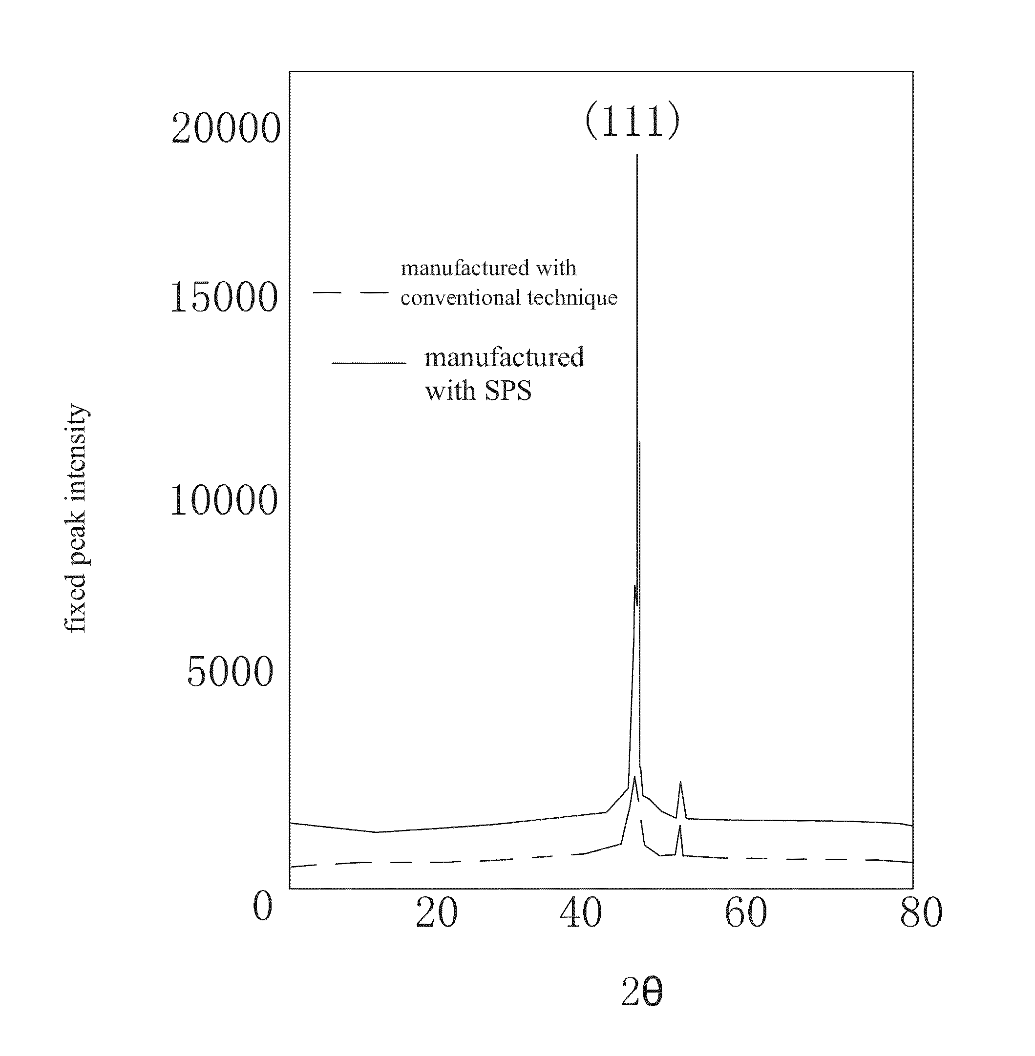
[0035]Referring to FIGS. 2-6, the present invention provides a method for manufacturing target material for a copper lead of a TFT-LCD (Thin-Film Transistor Liquid Crystal Display). The method comprises the following steps:

[0036]Step 1: providing copper powder and a spark plasma activated sintering device.

[0037]The mass of the copper powder can be calculated according to the predetermined surface area and thickness of a copper film to be formed with sputtering operation. The purity of the copper powder can be determined according to the properties of the copper film to be formed. In the instant embodiment, the purity of the copper powder is 99.99%.

[0038]Step 2: placing the copper powder in the spark plasma activated sintering device for sintering to obtain a target mat...


PUM

PropertyMeasurementUnit
temperatureaaaaaaaaaa
electrical resistivityaaaaaaaaaa

Abstract

The present invention relates to a method for manufacturing target material for copper lead of TFT-LCD array substrate and a target material. The method includes (1) providing copper powder and a spark plasma activated sintering device; and (2) placing the copper powder in the spark plasma activated sintering device for sintering to obtain a target material for manufacturing copper lead of TFT-LCD array substrate. The method for manufacturing target material for copper lead of TFT-LCD array substrate according to the present invention uses a spark plasma activated sintering device to sinter copper power for forming a target material. The process is simple and efficiency is high. Also, the orientation of crystalline plane of the target material can be effectively controlled to improve the performance of the target material, whereby a copper lead manufactured with such a target material shows low electrical resistivity, low film stress, and low surface roughness.

Description

BACKGROUND OF THE INVENTION[0001]1. Field of the Invention[0002]The present invention relates to the field of sputtering target, and in particular to a method for manufacturing target material for a copper lead of a TFT-LCD (Thin-Film Transistor Liquid Crystal Display) array substrate and a target material.[0003]2. The Related Arts[0004]Liquid crystal display (LCD) has a variety of advantages, such as thin device body, low power consumption, and being free of radiation, and is thus widely used. Most of the LCDs that are currently available in the market are backlighting LCDs, which comprise a liquid crystal display panel and a backlight module. The working principle of the liquid crystal display panel is that liquid crystal molecules are interposed between two parallel glass substrates and a plurality of vertical and horizontal fine electrical wires is arranged between the two glass substrates, whereby the liquid crystal molecules are controlled to change direction by application of...

Claims


Application Information

Patent Timeline
Patent Type & Authority Applications(United States)
IPC IPC(8): C23C14/34B22F3/105
CPCC23C14/3407B22F3/105B22F2003/1051C23C14/3414
Inventor KOU, HAO
Owner SHENZHEN CHINA STAR OPTOELECTRONICS TECH CO LTD
Why Eureka
Try Eureka