Eureka AIR delivers breakthrough ideas for toughest innovation challenges, trusted by R&D personnel around the world.

Semiconductor device package and method of manufacturing the same

Active Publication Date: 2021-08-12
ADVANCED SEMICON ENG INC
View PDF2 Cites 0 Cited by
  • Summary
  • Abstract
  • Description
  • Claims
  • Application Information

AI Technical Summary

Benefits of technology

The present patent text describes a semiconductor device package including two emitting devices. In some embodiments, the first emitting device has a larger coefficient of thermal expansion (CTE) than the second emitting device, meaning that it will expand and contract more easily with changes in temperature than the second emitting device. This can cause issues during manufacturing and use. To address this, the text describes a method where the second emitting devices are attached to the first emitting device, reducing the impact of the CTE differences. The technical effect is improved manufacturing stability and reliability of the semiconductor device package.

Problems solved by technology

Accordingly, separate manufacturing costs may be incurred for both components.
Furthermore, it may be difficult to reduce a size of the wireless communication device to attain a suitably compact product design.
However, due to the process limitation of the organic substrate, it is difficult to achieve fine-pitch (less than 15 / 15 μm), and the thickness of the organic substrate is relatively thick, which will hinder the miniaturization of the AiP system.

Method used


Image

  • Semiconductor device package and method of manufacturing the same
  • Semiconductor device package and method of manufacturing the same
  • Semiconductor device package and method of manufacturing the same

Examples


Embodiment Construction

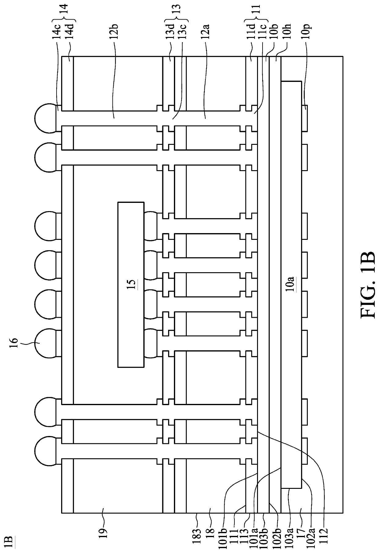
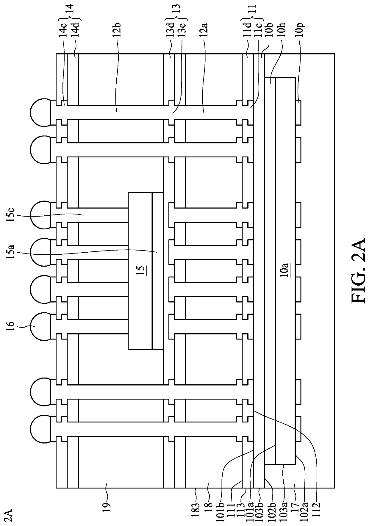
[0014]FIG. 1A illustrates a cross-sectional view of a semiconductor device package 1A in accordance with some embodiments of the present disclosure. The semiconductor device package 1A includes carriers 10a, 10b, circuit layers 11, 13, 14, interconnection structures 12a, 12b, an electronic component 15, electrical contacts 16 and package bodies 17, 18 and 19.

[0015]In some embodiments, the carrier 10a may be or include a glass substrate. In some embodiments, the carrier 10a may be or include an emitting device having one or more emitting components (e.g., an antenna, a light emitting device, a sensor or the like) disposed thereon. The carrier 10a may include conductive pad(s), trace(s), and interconnection(s) (e.g. via(s)). In some embodiments, the carrier 10a may include transparent material. In some embodiments, the carrier 10a may include opaque material. The carrier 10a includes a material having a dielectric constant (Dk) less than approximately 5. The carrier 10a includes a mat...


PUM


Abstract

A semiconductor device package includes a first circuit layer, a first emitting device and a second emitting device. The first circuit layer has a first surface and a second surface opposite to the first surface. The first emitting device is disposed on the second surface of the first circuit layer. The first emitting device has a first surface facing the first circuit layer and a second surface opposite to the first surface. The first emitting device has a first conductive pattern disposed on the first surface of the first emitting device. The second emitting device is disposed on the second surface of the first emitting device. The second emitting device has a first surface facing the second surface of the first emitting device and a second surface opposite to the first surface. The second emitting device has a second conductive pattern disposed on the second surface of the emitting device. A coefficient of thermal expansion (CTE) of the first emitting device is greater than a CTE of the second emitting device.

Description

BACKGROUND1. Technical Field[0001]The present disclosure relates to a semiconductor device package and a method of manufacturing the same, and more particularly to a semiconductor device package including an antenna and a method of manufacturing the same.2. Description of the Related Art[0002]Wireless communication devices, such as cell phones, typically include antennas for transmitting and receiving radio frequency (RF) signals. Comparably, a wireless communication device includes an antenna and a communication module, each disposed on different parts of a circuit board. Under the comparable approach, the antenna and the communication module are separately manufactured and electrically connected together after being placed on the circuit board. Accordingly, separate manufacturing costs may be incurred for both components. Furthermore, it may be difficult to reduce a size of the wireless communication device to attain a suitably compact product design. To reduce the cost and packag...

Claims


Application Information

Patent Timeline
IPC IPC(8): H01L23/66H01L23/00H01L23/373H01L21/768
CPCH01L23/66H01L24/29H01L2223/6677H01L21/768H01L23/3731H01L23/49816H01L23/49827H01L23/49838H01L23/3121H01L21/561H01Q1/2283H01L23/5389H01L23/5383H01L23/5384H01L23/15H01L23/5385H01L2224/16225H01L2224/81801H01L2224/13101H01L2924/181H01L24/13H01L24/16H01L24/81H01L23/562H01L21/6835H01L2221/68345H01L2224/16235H01L24/19H01L24/20H01L2224/73267H01L24/73H01L25/16H01L2924/00014H01L2924/014H01L2924/00012
Inventor HSIEH, MENG-WEIKANG, KUO-CHANG
Owner ADVANCED SEMICON ENG INC
Why Eureka
Eureka Blog
Learn More