Method of manufacturing semiconductor device

a manufacturing method and semiconductor technology, applied in semiconductor devices, electrical equipment, electric discharge tubes, etc., can solve the problems of difficult formation of openings in protective films between the cap layer and the electron supply layer, deterioration of electrical properties, etc., to enhance the effect of enhancing the etching selectivity ratio of the nitride layer

Active Publication Date: 2021-08-19
SUMITOMO ELECTRIC IND LTD +1
View PDF0 Cites 0 Cited by
  • Summary
  • Abstract
  • Description
  • Claims
  • Application Information

AI Technical Summary

Benefits of technology

[0009]It is an object of the present disclosure to provide a method of manufacturing a semiconductor device that can enhance the etching selectivity ratio of a nitride layer containing silicon to a nitride layer containing gallium without the use of a fluorine-based gas.
[0010]According to the present disclosure, a method of manufacturing a semiconductor device including a substrate; a first nitride layer containing gallium on the substrate; and a second nitride layer containing silicon on the first nitride layer, includes: generating an etchant of a gas containing chlorine atoms or bromine atoms; and selectively removing the second nitride layer with respect to the first nitride layer by the etchant, wherein in the generating the etchant, the etchant is generated by plasma discharge of the gas, wherein in the selectively removing the second nitride layer, the second nitride layer and the first nitride layer are prevented from being irradiated with ultraviolet rays generated at a time of the plasma discharge, and wherein the selectively removing the second nitride layer includes etching the second nitride layer under a first atmosphere at a first pressure that is lower than a first saturated vapor pressure of a silicon compound containing silicon atoms and chlorine atoms or bromine atoms contained in the gas and that is higher than a second saturated vapor pressure of a gallium compound containing gallium atoms and chlorine atoms or bromine atoms contained in the gas.
[0011]According to the present disclosure, it is possible to provide a method of manufacturing a semiconductor device that can enhance the etching selectivity ratio of a nitride layer containing silicon to a nitride layer containing gallium without the use of a fluorine-based gas.

Problems solved by technology

A residue of fluorine in the nitride semiconductor layer may cause deterioration of electrical properties due to fluctuation in threshold voltage or the like.
Except etching using plasma of fluorine-based gas, it is difficult to form an opening in a protective film on the cap layer and the electron supply layer, which are made thinner, at a high etching selectivity ratio.

Method used


Image

  • Method of manufacturing semiconductor device
  • Method of manufacturing semiconductor device
  • Method of manufacturing semiconductor device

Examples


Embodiment Construction

[0027]In the following, an embodiment for carrying out will be described.

Description of Embodiment of the Present Disclosure

[0028]To begin with, aspects of the present disclosure are listed and described below. In the following description, the same reference characters are allotted to the same or corresponding elements and the same descriptions thereof are not repeated.

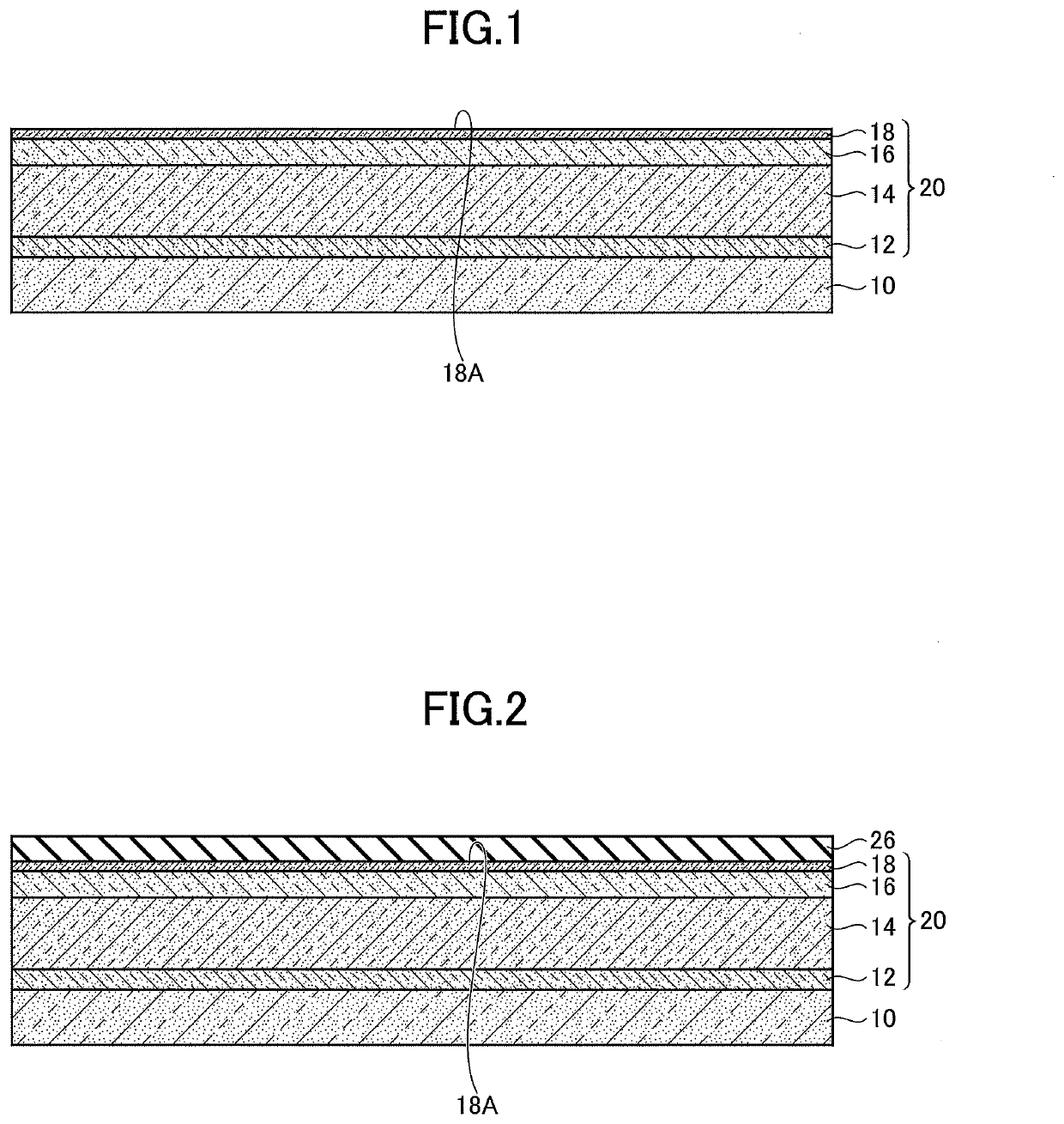
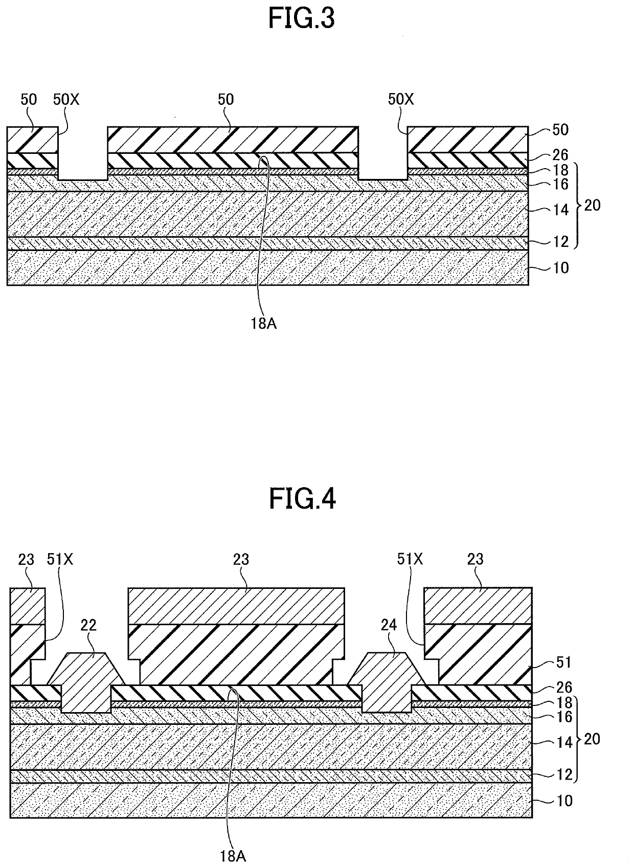
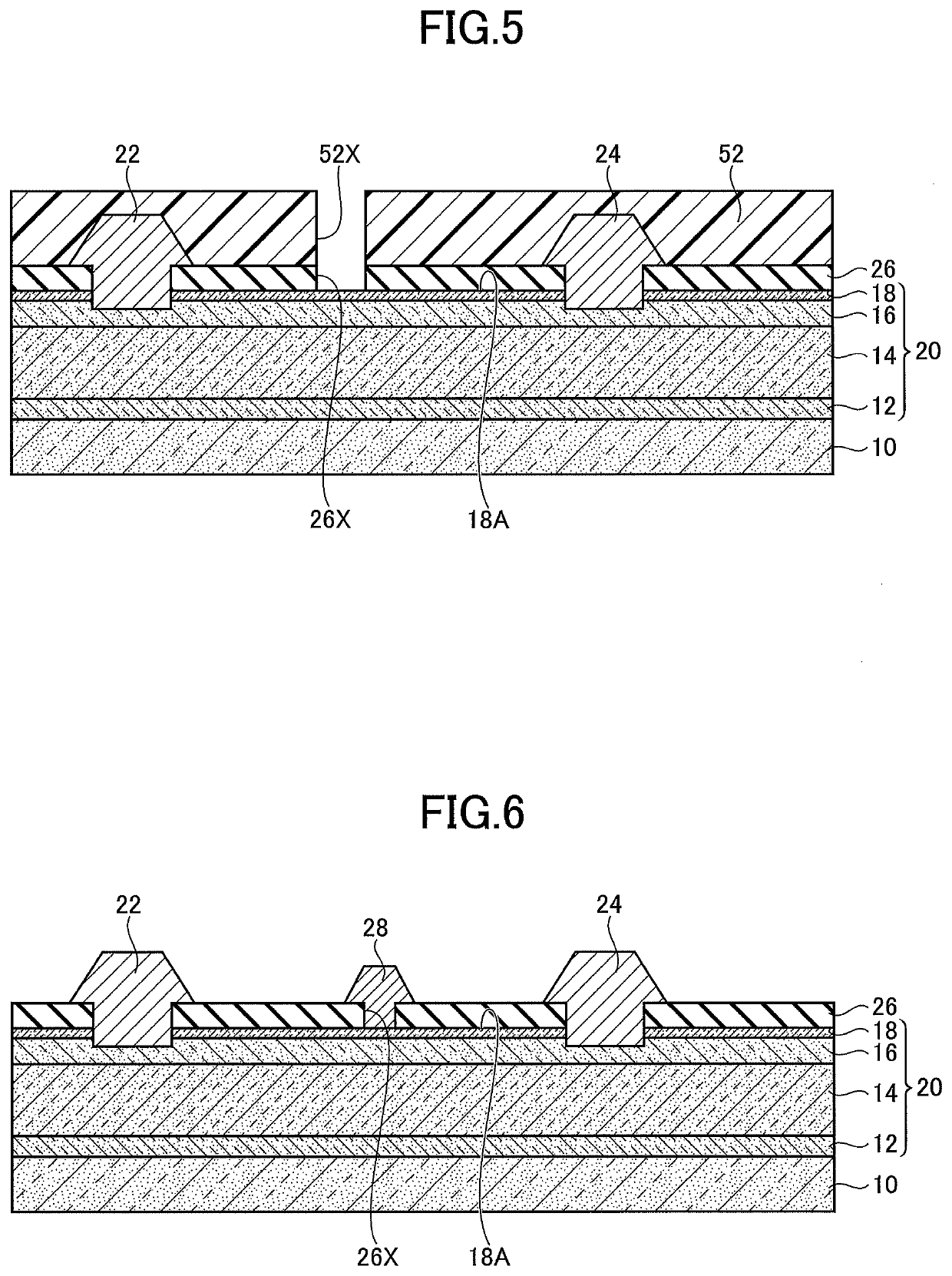
[0029] According to one aspect of the present disclosure, a method of manufacturing a semiconductor device including a substrate; a first nitride layer containing gallium on the substrate; and a second nitride layer containing silicon on the first nitride layer includes: generating an etchant of a gas containing chlorine atoms or bromine atoms; and selectively removing the second nitride layer with respect to the first nitride layer by the etchant, wherein in the generating the etchant, the etchant is generated by plasma discharge of the gas, wherein in the selectively removing the second nitride layer, the second ni...


PUM

PropertyMeasurementUnit
pressureaaaaaaaaaa
pressureaaaaaaaaaa
thicknessaaaaaaaaaa

Abstract

A method of manufacturing a semiconductor device including a substrate; a first nitride layer containing gallium on the substrate; and a second nitride layer containing silicon on the first nitride layer includes generating an etchant of a gas containing chlorine atoms or bromine atoms; and selectively removing the second nitride layer, wherein the etchant is generated by plasma discharge of the gas, wherein the second nitride layer and the first nitride layer are prevented from being irradiated with ultraviolet rays generated at a time of the plasma discharge, and wherein the selectively removing the second nitride layer includes etching the second nitride layer under a first atmosphere at a first pressure that is lower than a first saturated vapor pressure of a silicon compound and that is higher than a second saturated vapor pressure of a gallium compound.

Description

CROSS-REFERENCE TO RELATED APPLICATION[0001]The present application is based upon and claims priority to Japanese Patent Application No. 2020-026568, filed on Feb. 19, 2020, the entire contents of which are incorporated herein by reference.BACKGROUND OF THE INVENTION1. Field of the Invention[0002]The present disclosure relates to a method of manufacturing a semiconductor device.2. Description of the Related Art[0003]As a type of semiconductor device, a high electron mobility transistor (HEMT) using a gallium nitride (GaN)-based nitride semiconductor is known. In manufacturing a HEMT using a GaN-based nitride semiconductor (which may be referred to as a GaN-HEMT hereinafter), a protective film of silicon nitride (SiN) is formed on the nitride semiconductor layer, an opening is formed in the protective film by etching using plasma of fluorine-based gas, and a gate electrode is formed in the opening (for example, Patent Document 1).PRIOR ART DOCUMENTSPatent Documents[0004][Patent Docum...

Claims


Application Information

Patent Timeline
Patent Type & Authority Applications(United States)
IPC IPC(8): H01L21/311H01L21/02H01L21/28
CPCH01L21/31116H01L21/0254H01L29/66462H01L21/28H01L21/0217H01L21/3065H01L29/7787H01L29/2003H01L29/41766H01J37/32357H01J37/32422H01J37/32651H01L21/28575H01L21/28581H01L21/28587
Inventor SUGAWARA, KENTASAMUKAWA, SEIJIOHORI, DAISUKE
Owner SUMITOMO ELECTRIC IND LTD
Why Eureka
Try Eureka