Method for argon plasma induced ultraviolet light curing step for increasing silicon-containing photoresist selectivity

a technology of argon plasma and photoresist layer, applied in the field of lithography, can solve the problems of insufficient improvement of etch resistance, difficult to accurately perform etching operations, and more critical lithography techniques to pattern holes or trenches in the dielectric, so as to increase the selectivity ratio of the underlying photoresist layer, improve etch profile control, and increase the effect of selectivity

Inactive Publication Date: 2007-01-09
LAM RES CORP
View PDF9 Cites 17 Cited by
  • Summary
  • Abstract
  • Description
  • Claims
  • Application Information

AI Technical Summary

Benefits of technology

[0016]The advantages of the present invention are numerous. Most notably, the formation of the hardened layer increases the selectivity ratio of the underlying photoresist layer or interlayer dielectric relative to the hardened layer of the top photoresist layer. Accordingly, any etch processes performed on the substrate with the hardened layer will etch through the underlying photoresist layer or interlayer dielectric at an increased rate relative to the etch rate of the hardened layer. Furthermore, the etch profile control will be improved as a result of the increased selectivity, thereby allowing for pinpoint accuracy as semiconductor feature size continues to shrink. Additionally, an etch chamber may be utilized for curing the hardened layer. As a result, after the curing process, the substrate may be etched in the same chamber. Hence, throughput is increased and handling of the substrate is minimized.

Problems solved by technology

Sharp lithographic transmission becomes more of a challenge as wafers progress to higher density chips with shrinking geometries.
Furthermore, as metallization transitions to dual damascene processes, lithography techniques to pattern holes or trenches in the dielectric become more critical.
Moreover, as device features progressively become smaller, the aspect ratios for those same features become greater, thereby making it more difficult to accurately perform etching operations.
However, resist compositions containing silicon, either in the main resist polymer or by post-exposure surface treatment (e.g., silylation), have either failed to deliver adequate improvement in etch resistance or have had poor processing performance due to the unacceptable selectivity past the silicon containing layer.

Method used


Image

  • Method for argon plasma induced ultraviolet light curing step for increasing silicon-containing photoresist selectivity
  • Method for argon plasma induced ultraviolet light curing step for increasing silicon-containing photoresist selectivity
  • Method for argon plasma induced ultraviolet light curing step for increasing silicon-containing photoresist selectivity

Examples


Embodiment Construction

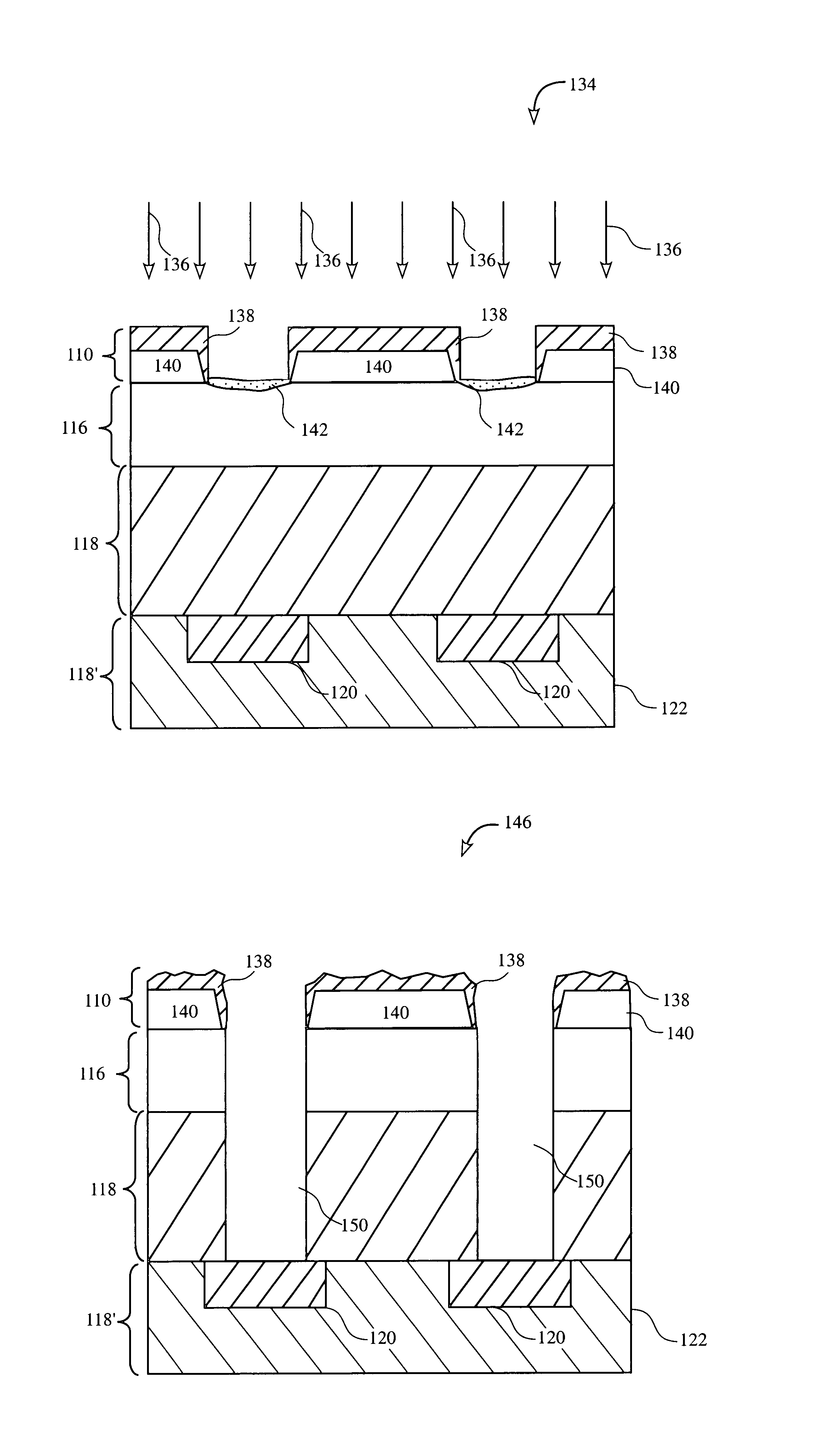
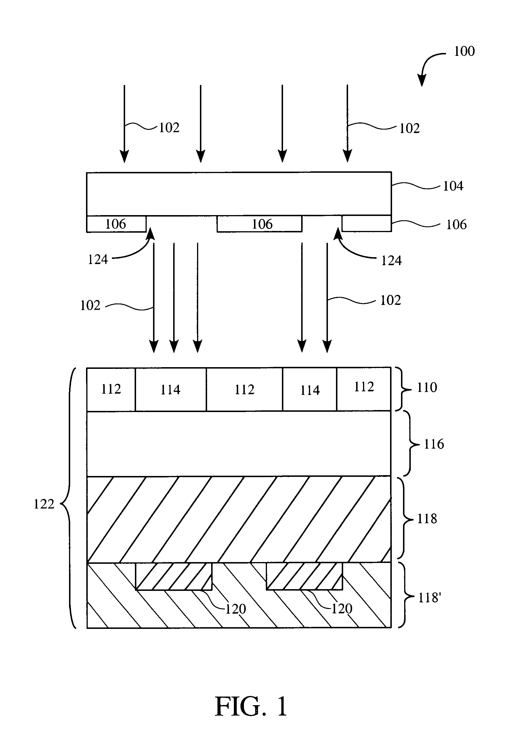
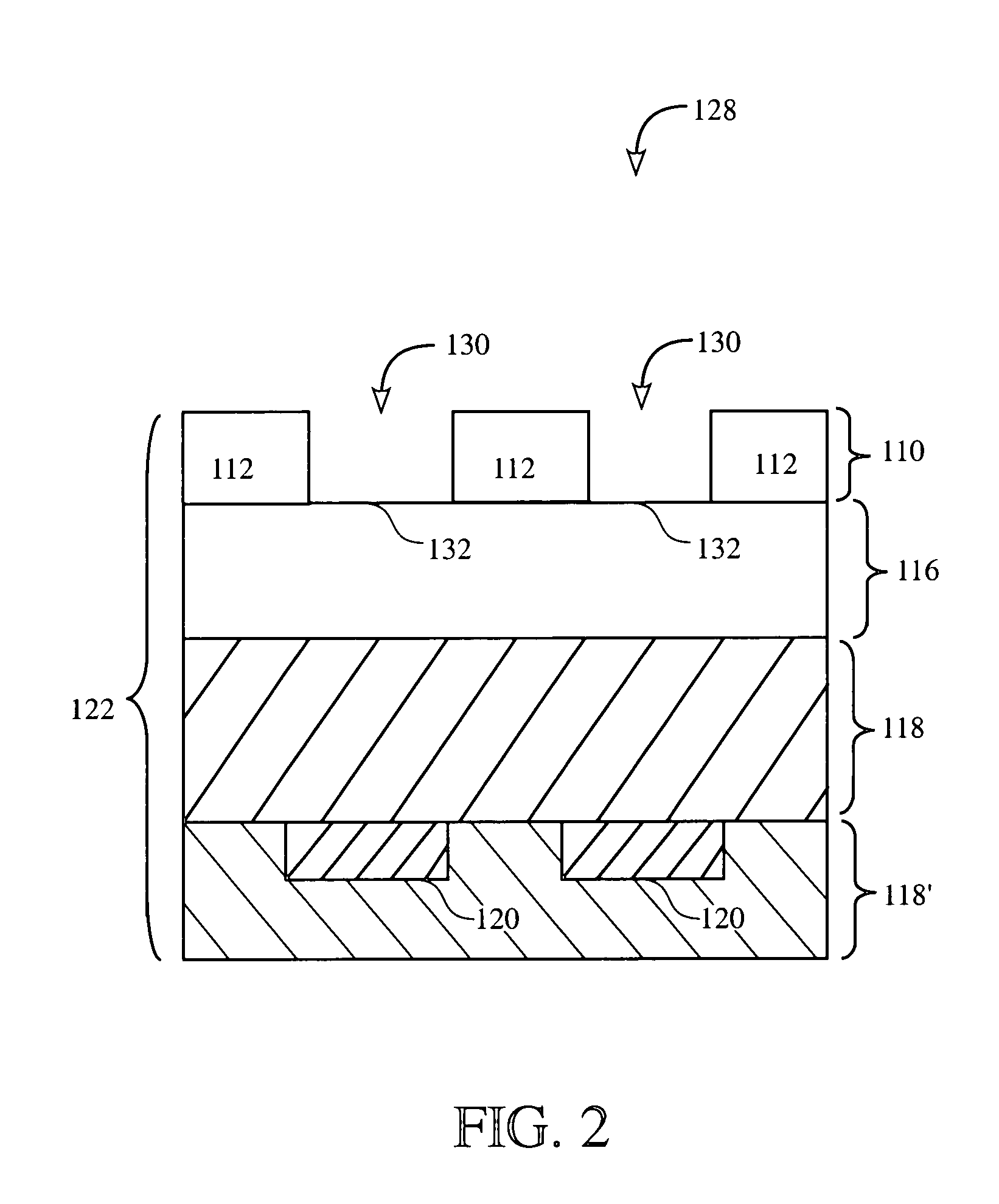
[0024]An invention is described for an apparatus and a method for enhancing the selectivity of a silicon containing photoresist thereby improving etch profile control. It will be obvious, however, to one skilled in the art, that the present invention may be practiced without some or all of these specific details. In other instances, well known process operations have not been described in detail in order not to unnecessarily obscure the present invention.

[0025]The embodiments of the present invention provide an apparatus and method for an improved selectivity of a silicon-containing photoresist which in turn, allows for amelioration of a subsequent etch profile. In one embodiment, a hardened layer is formed in a silicon-containing photoresist by exposing the developed silicon-containing photoresist to ultraviolet (UV) light. In accordance with one embodiment of the invention, the UV light is generated by striking a plasma containing an inert gas such as neon, as will be described be...


PUM

PropertyMeasurementUnit
temperatureaaaaaaaaaa
pressureaaaaaaaaaa
pressureaaaaaaaaaa

Abstract

A method for increasing etching selectivity of a developed silicon-containing photoresist layer on a non-silicon containing photoresist layer on a substrate. The developed silicon-containing photoresist layer includes polymer chains containing silicon. Next, the developed silicon-containing photoresist layer and uncovered portions of the non-silicon containing photoresist layer are exposed to an ultraviolet (UV) light, where the UV light emanates from a UV generating agent, such as neon, xenon, helium, hydrogen, or krypton gas in an inert gas (e.g., argon, etc.) plasma. A top portion of the developed silicon-containing photoresist layer is then converted to a hardened layer, where the hardened layer is created by cross-linking the polymer chains containing silicon and the cross-linking is activated by the UV light. Next, an etch is performed on the uncovered portions of the non-silicon containing photoresist layer and the substrate using the hardened layer.

Description

CROSS REFERENCE TO RELATED APPLICATIONS[0001]This application is related to U.S. Pat. No. 6,541,361, filed on the same day as the instant application and entitled “PLASMA ENHANCED METHOD FOR INCREASING SILICON-CONTAINING PHOTORESIST SELECTIVITY.” This application is hereby incorporated by reference.BACKGROUND OF THE INVENTION[0002]1. Field of the Invention[0003]This invention relates generally to lithography and more particularly to a method and apparatus for increasing the selectivity of a silicon-containing photoresist layer to improve profile control of etched features without decreasing wafer throughput.[0004]2. Description of the Related Art[0005]The ability to work selectively on small well defined areas of a substrate is paramount in the manufacture of semiconductor devices. In the continuing quest to achieve higher levels of performance and higher functional density of the semiconductor devices, the microelectronics industry is committed to applying new processes to further ...

Claims


Application Information

Patent Timeline
Patent Type & Authority Patents(United States)
IPC IPC(8): G03F7/40G03F7/20G03F7/36G03F7/075G03F7/09
CPCG03F7/40G03F7/075G03F7/094
Inventor KO, FRANCISCHEN, RICHARDLEE, CHARLIE
Owner LAM RES CORP
Why Eureka
Try Eureka