Supercharge Your Innovation With Domain-Expert AI Agents!

Semiconductor Strain Gauge and Method for Manufacturing Same

a technology of micro-semiconductor and strain gauge, which is applied in the direction of instruments, device details, and piezoelectric/electrostrictive device details, etc., can solve the problems of high yield loss and cost, poor uniform thickness across the wafer, and complicated post-fabrication and packaging steps

Inactive Publication Date: 2021-08-19
ADVANCED NANOSTRUCTURES LLC
View PDF3 Cites 3 Cited by
  • Summary
  • Abstract
  • Description
  • Claims
  • Application Information

AI Technical Summary

Benefits of technology

This approach results in high-yield, uniformly thick strain gages with improved resistance consistency and simplified post-fabrication processing, enabling efficient handling and packaging of semiconductor strain gages.

Problems solved by technology

However, the post fabrication and packaging steps become more complicated because smaller sensors are more difficult to handle.
The current methods of bulk manufacturing strain gages present a major disadvantage in achieving a uniform thickness of sensors across a given wafer, resulting in higher yield loss and cost.
One drawback of currently available strain gages is that when conventional manufacturing techniques are applied, the uniformity in thickness is in general poor across the wafer.
Furthermore, once the sensors are fabricated on a wafer, the singulation of individual sensors is difficult because of their small size.
Current methods require picking individual sensors out of a solution, which is difficult and time consuming.

Method used


Image

  • Semiconductor Strain Gauge and Method for Manufacturing Same
  • Semiconductor Strain Gauge and Method for Manufacturing Same
  • Semiconductor Strain Gauge and Method for Manufacturing Same

Examples


Embodiment Construction

[0023]The current invention is now described with reference to the figures. Components appearing in more than one figure bear the same reference numerals.

[0024]Preferred embodiments of the present invention are described herein. Other variations of the present invention may also be performed and are claimed in the present patent, as referenced herein. The invention is described in combination with particular embodiments, but it is not the intention to limit the invention to the described embodiments. Rather, it is intended to encompass alternatives, equivalents and modifications as described by the scope of the presented claims.

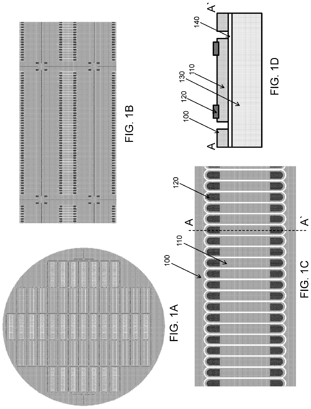
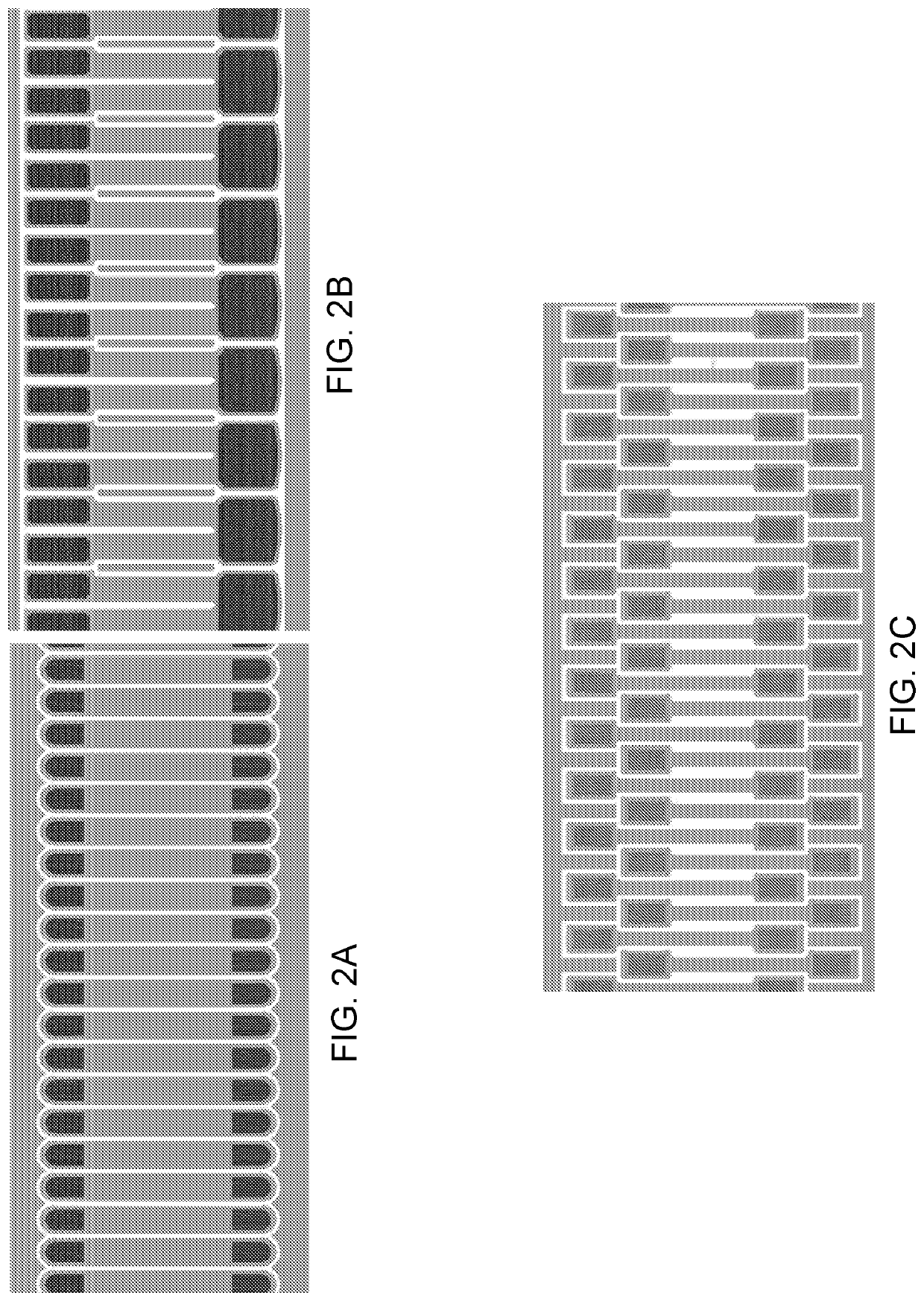
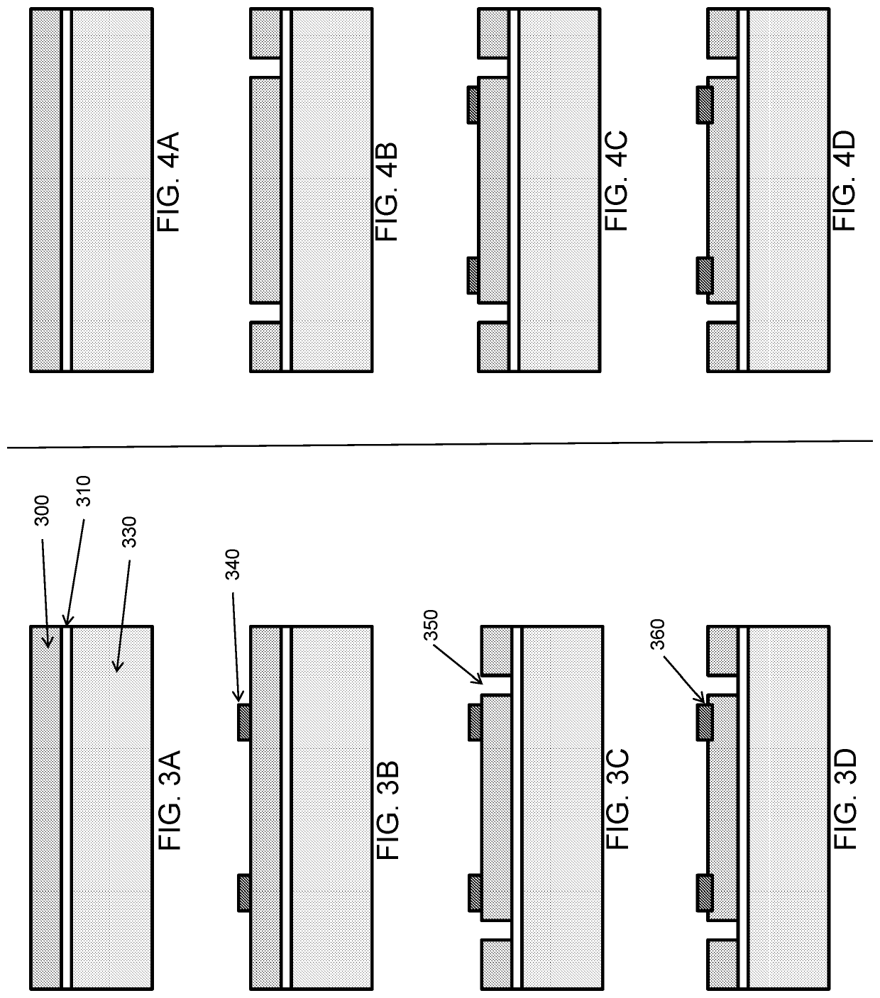
[0025]Typically, when fabricating semiconductor devices, many devices are fabricated on one wafer. As devices become smaller, and thus typically cheaper, it becomes more difficult to free the devices from the wafer in a clean and high yielding way once the fabrication is finished. This invention describes a method of making high yielding semiconductor strain ...


PUM

PropertyMeasurementUnit
temperatureaaaaaaaaaa
resistanceaaaaaaaaaa
piezo resistance effectaaaaaaaaaa

Abstract

Semiconductor strain gages fabricated on Silicon-on-insulator (SOI) material, and the method of making them. Force sensing elements are uniformly batch-fabricated at wafer level and singulated individually by a wire bonding method. In another method, they are singulated by plucking them off the wafer from their attachment site.

Description

RELATED APPLICATIONS[0001]This patent application is a continuation of U.S. patent application Ser. No. 15 / 592,796, filed May 11, 2017, the entirety of which is incorporated by reference.FIELD OF THE INVENTION[0002]The present invention relates to semiconductor strain gages. More particularly, the present invention relates to semiconductor strain gages fabricated on Silicon-oninsulator (SOI) material, and the method of making such gages.BACKGROUND OF THE INVENTION[0003]Objects subject to external forces undergo strain. In numerous circumstances, it is desirable to know the strain a particular object is experiencing in order to preserve the structural integrity of the object, and / or the overall device of which the object is a part. Examples include automobile parts, airplane parts, highway and bridge components, railway components and components of devices used in the aerospace industry.[0004]An object experiencing strain will typically experience a deformation in its shape. Strain g...

Claims


Application Information

Patent Timeline
Patent Type & Authority Applications(United States)
IPC IPC(8): H01L41/22G01L1/18G01L1/22H01L41/047H01L41/08H01L41/04H10N30/01H10N30/00H10N30/80H10N30/87
CPCH01L41/22G01L1/18G01L1/2293H01L41/0472H01L41/0471H01L41/04H01L41/047H01L41/08H01L41/0805H10N30/01H10N30/87H10N30/871H10N30/872H10N30/704
Inventor OKULAN, NIHAT
Owner ADVANCED NANOSTRUCTURES LLC
Features
  • R&D
  • Intellectual Property
  • Life Sciences
  • Materials
  • Tech Scout
  • Unparalleled Data Quality
  • Higher Quality Content
  • 60% Fewer Hallucinations
Learn More