Semiconductor device and control method thereof

Active Publication Date: 2021-09-09
HONDA MOTOR CO LTD +1
View PDF0 Cites 0 Cited by
  • Summary
  • Abstract
  • Description
  • Claims
  • Application Information

AI Technical Summary

Benefits of technology

The present invention simplifies the configuration of a semiconductor device and a control method thereof, by replacing a memory block that has malfunctions and all the memory blocks in the same area. The addresses of the memory blocks are made common between semiconductor chips, reducing the number of circuits needed to select the appropriate memory block for input / output. This simplifies the overall configuration of the semiconductor device and improves its efficiency.

Problems solved by technology

When a plurality of selection circuits are provided, the semiconductor device increases in size, the circuit configuration becomes complicated, variation occurs in speed of input / output to / from the memory block, and delay is likely to occur.

Method used


Image

  • Semiconductor device and control method thereof
  • Semiconductor device and control method thereof
  • Semiconductor device and control method thereof

Examples


Embodiment Construction

[0020]Hereinafter, a semiconductor device and a control method thereof according to an embodiment to which the present invention is applied will be described in detail with reference to the drawings. In the drawings used in the following description, there are cases in which characteristic portions are appropriately enlarged for convenience of illustration so that characteristics of the present invention can be easily understood, and dimensional proportions and the like between respective constituent elements may not be the same as the actual ones. Also, materials, dimensions, and the like illustrated in the following description are merely examples, and the present invention is not limited thereto and can be implemented with appropriate modifications within a range not changing the gist of the present invention.

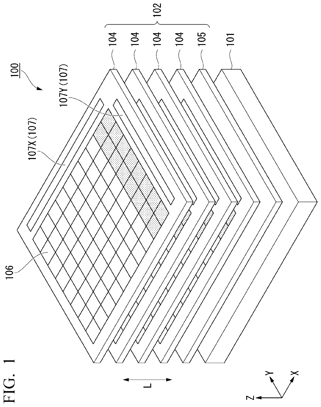
[0021]FIG. 1 is a perspective view schematically illustrating a configuration example of a semiconductor device 100 according to a first embodiment of the present invention....


PUM


Abstract

A semiconductor device according to the present invention is formed by a plurality of semiconductor chips laminated on a substrate which are connected via a through electrode penetrating in a lamination direction, in which the plurality of semiconductor chips include first semiconductor chips 104 each having memory blocks and a decoder and a second semiconductor chip having a logic circuit, the logic circuit includes one selection circuit connected to the decoder of all the first semiconductor chips 104 and configured to select addresses of a first memory block 106A that stops input / output and a second memory block 106B that performs input / output instead among the plurality of memory blocks, and the addresses of the selected first memory block 106A and the selected second memory block 106B are each common to all the first semiconductor chips.

Description

BACKGROUND OF THE INVENTIONField of the Invention[0001]The present invention relates to a semiconductor device and a control method thereof.[0002]Priority is claimed on Japanese Patent Application No. 2020-038815, filed in Japan on Mar. 6, 2020, the content of which is incorporated herein by reference.Description of Related Art[0003]In recent years, a high bandwidth memory (HBM), in which DRAM chips are laminated to expand a bandwidth and increase a speed, has attracted attention (Patent Documents 1 and 2). The most advanced HBM2 currently being developed is made by laminating four chips and has input / output I / Os for 1024 channels. In order to adapt to the speed of a CPU / GPU whose speed is further increased, in HBMs to be developed in the future, the number of input / output I / Os needs to be increased by one or two digits in some way to realize larger-scale parallel processing (parallelism).[0004]In order to realize large-scale parallel processing in which the number of input / output I...

Claims


Application Information

Patent Timeline
IPC IPC(8): G11C11/408H01L25/18H01L23/48G11C11/4096
CPCG11C11/4087G11C11/4096H01L23/481H01L25/18G11C5/025G11C29/76G11C29/4401H01L25/0657H01L2225/06513H01L2225/06541H01L24/32H01L24/08H01L2224/08145H01L2224/32145H01L2224/33181H01L2224/09181H01L24/09H01L24/33H01L2924/00015H01L2224/16H01L2224/16145
Inventor SAKUI, KOJIOHBA, TAKAYUKI
Owner HONDA MOTOR CO LTD
Why Eureka
Try Eureka