Interconnect networks using microled-based optical links

a technology of optical links and interconnect networks, applied in the direction of optical elements, electromagnetic transceivers, instruments, etc., can solve the problems of increasing the cost of per-transistor, reducing the yield, and dramatically reducing the benefits of further transistor shrinkag

Pending Publication Date: 2021-10-14
AVICENATECH CORP
View PDF10 Cites 4 Cited by
  • Summary
  • Abstract
  • Description
  • Claims
  • Application Information

AI Technical Summary

Benefits of technology

[0014]These and other aspects of the invention are...

Problems solved by technology

However, the benefits of further transistor shrinks are decreasing dramatically as decreasing marginal performance benefits combine with decreased yields and increased per-transistor costs.
Independent of these limitations, a single IC can only contain so much functionality, and...

Method used


Image

  • Interconnect networks using microled-based optical links
  • Interconnect networks using microled-based optical links
  • Interconnect networks using microled-based optical links

Examples


Embodiment Construction

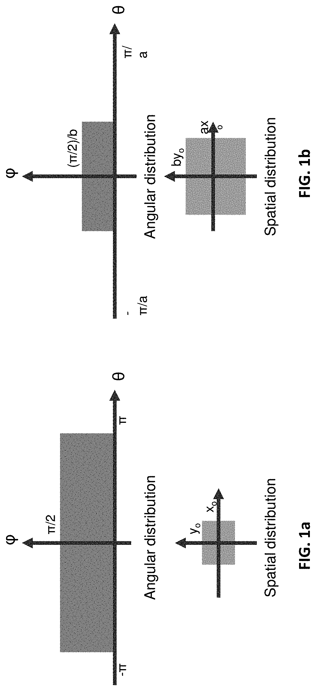
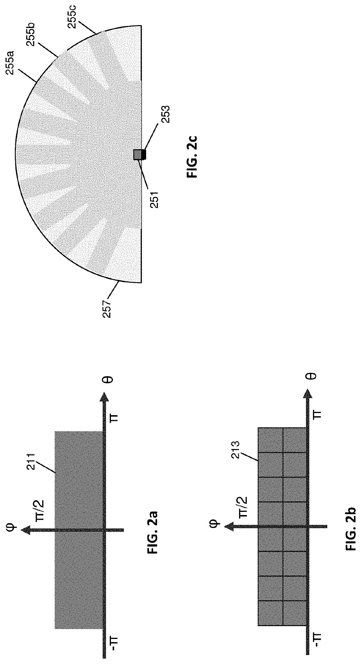
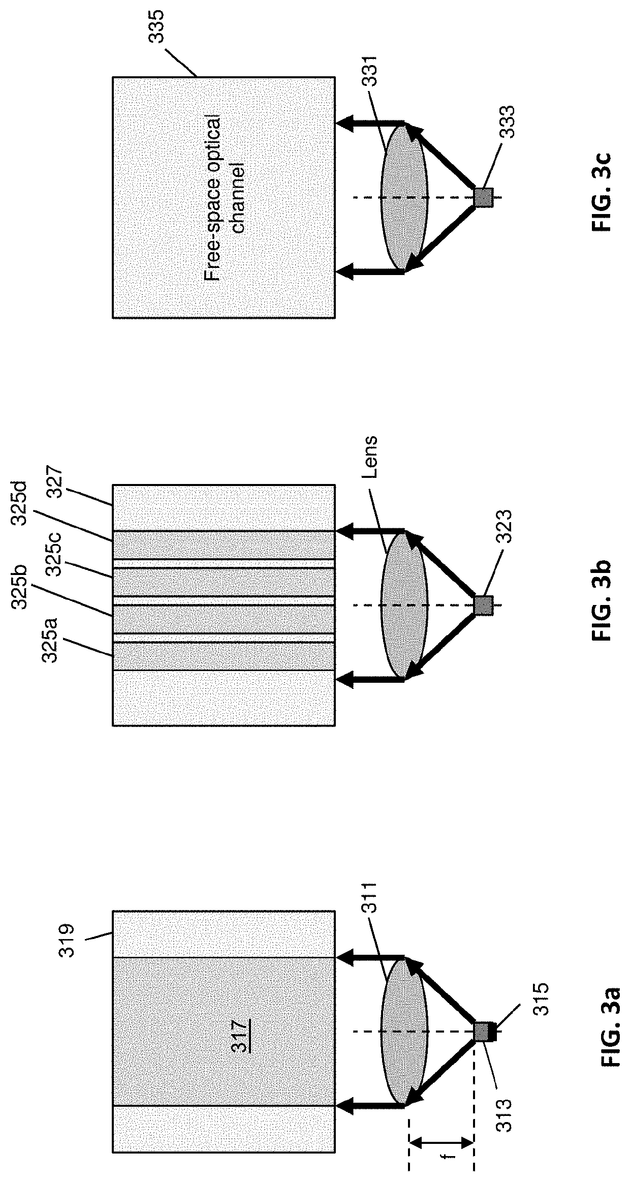
lass="d_n">[0085]In some embodiments parallel optical links (POLs) use microLED sources and photodetectors, which may be collectively referred to as optoelectronic (OE) devices. POLs provide highly parallel, low latency point-to-point connectivity. Some embodiments may also or instead provide for point-to-multipoint connectivity.

[0086]A microLED is made from a p-n junction of a direct-bandgap semiconductor material. A microLED is distinguished from a semiconductor laser (SL) in the following ways: (1) a microLED does not have an optical resonator structure; (2) the optical output from a microLED is almost completely spontaneous emission whereas the output from a SL is dominantly stimulated emission; (3) the optical output from a microLED is temporally and spatially incoherent whereas the output from a SL has significant temporal and spatial coherence; (4) a microLED is usually designed to be operated down to a zero minimum current, whereas a SL is designed to be operated above a min...


PUM


Abstract

Integrated circuit chips may be optically interconnected using microLEDs. Some interconnections may be vertically-launched parallel optical links. Some interconnections may be planar-launched parallel optical links.

Description

CROSS REFERENCE TO RELATED APPLICATION[0001]This application claims the benefit of the filing date of U.S. Provisional Patent Application No. 63 / 009,199, filed on Apr. 13, 2020, the disclosure of which is incorporated by reference herein.BACKGROUND OF THE INVENTION[0002]Demands for increased computing and networking performance are seemingly ubiquitous and never ending. Prominent applications include data center servers, high-performance computing clusters, artificial neural networks, and network switches.[0003]For decades, dramatic integrated circuit (IC) performance and cost improvements were driven by shrinking transistor dimensions combined with increasing die sizes, summarized in the famous Moore's Law. Transistor counts in the billions have allowed consolidation onto a single system-on-a-chip (SoC) of functionality that was previously fragmented across multiple ICs.[0004]However, the benefits of further transistor shrinks are decreasing dramatically as decreasing marginal perf...

Claims


Application Information

Patent Timeline
IPC IPC(8): H04B10/80H01L33/00H04B10/40G02B6/43
CPCH04B10/803H01L33/0045H01L33/10G02B6/43H04B10/40H01L25/0753H01L33/58H01L33/60G02B6/4214H04B10/27H04J14/0217H04B10/25
Inventor KALMAN, ROBERTPEZESHKI, BARDIATSELIKOV, ALEXANDERDANESH, CAMERON
Owner AVICENATECH CORP
Why Eureka
Try Eureka