OLED display panel and driving method thereof

a technology of light-emitting diodes and display panels, applied in the field of displays, can solve problems such as drift of threshold voltage, non-uniform display, and insatisfactory display uniformity of panels

Active Publication Date: 2021-10-28
SHENZHEN CHINA STAR OPTOELECTRONICS SEMICON DISPLAY TECH CO LTD
View PDF0 Cites 0 Cited by
  • Summary
  • Abstract
  • Description
  • Claims
  • Application Information

AI Technical Summary

Benefits of technology

[0043]Advantages of the present disclosure are as follows. An OLED display panel of the present disclosure includes a plurality of pixel unit circuits and an external compensation unit connected to all of the pixel unit circuits. The external compensation unit performs external compensation on each of the pixel unit circuits, obtains an initial threshold voltage of a corresponding driving TFT of each of the pixel unit circuits, adds the initial threshold voltage to a predetermined initial potential, and then inputs a sum of the initial threshold voltage and the predetermined initial potential to each of the pixel unit circuits. Each of the pixel unit circuits performs internal compensation based on the sum of the initial threshold voltage and the predetermined initial potential. That is, the external compensation and the internal compensation are combined. The external compensation can compensate for a non-uniform...

Problems solved by technology

A positive or negative drift of the threshold voltage cause different currents to flow through the OLED under the same data signal, resulting in a problem of display non-uniformity.
For example, factors such as irradiation of oxide semiconductor and voltage stress effects of source and drain electrodes may cause the drift of the threshold voltage.
As a result, a current flowing through the OLED is inconsi...

Method used


Image

  • OLED display panel and driving method thereof
  • OLED display panel and driving method thereof
  • OLED display panel and driving method thereof

Examples


Embodiment Construction

[0052]In order to further describe technical means used by the present disclosure and effects thereof, preferred embodiments of the present disclosure are described in detail below in conjunction with the drawings thereof.

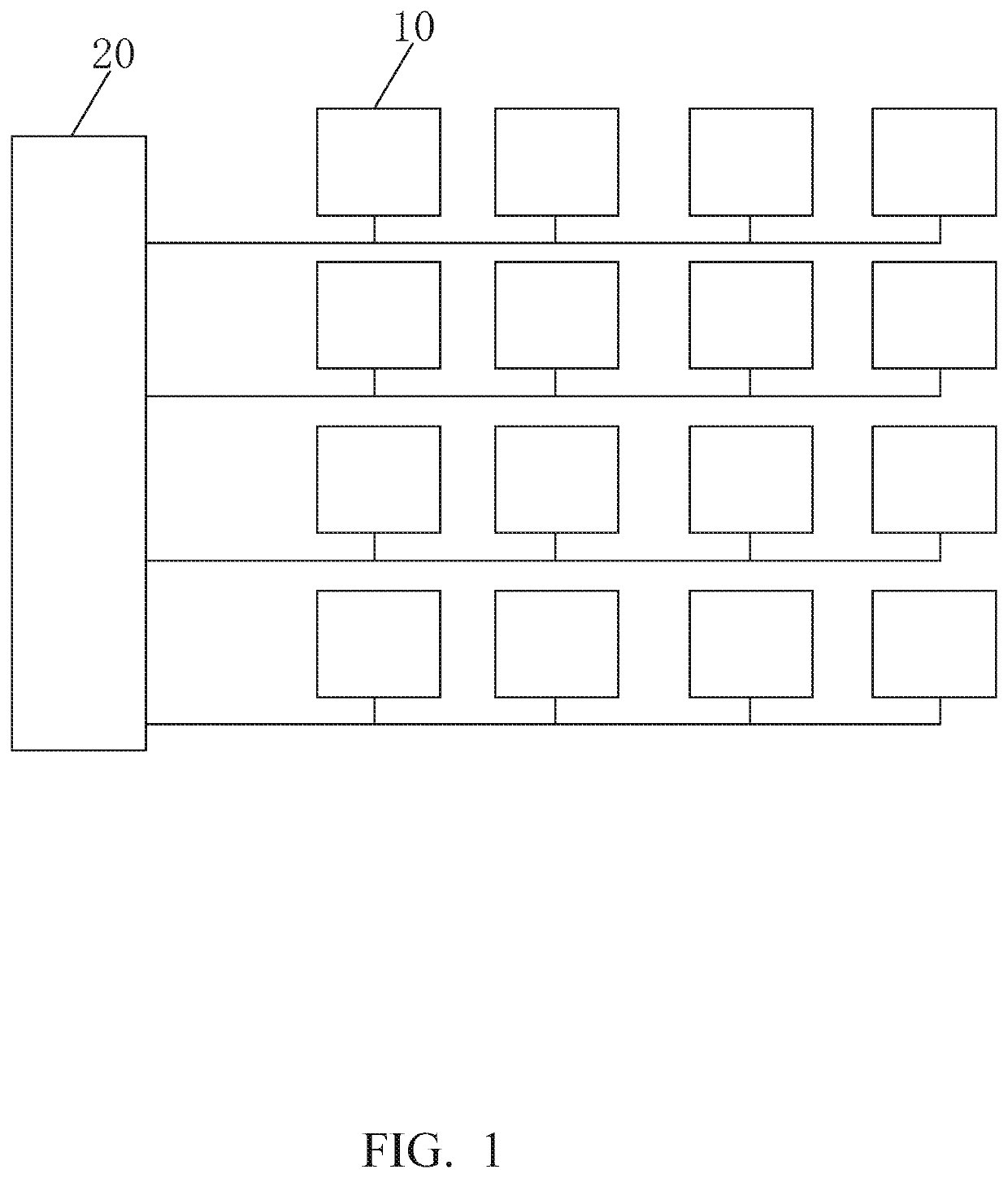
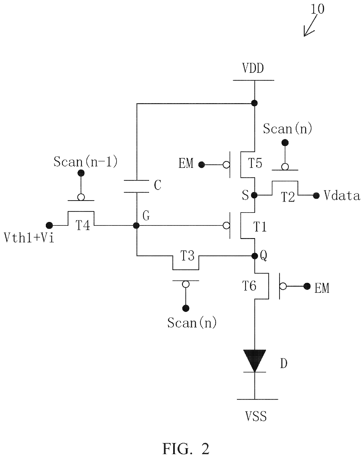
[0053]Referring to FIG. 1, the present disclosure provides an organic light emitting diode (OLED) display panel including: a plurality of pixel unit circuits 10 and an external compensation unit 20 connected to all of the pixel unit circuits 10.

[0054]The external compensation unit 20 is configured to perform external compensation on each of the pixel unit circuits 10, obtain an initial threshold voltage Vth1 of a corresponding driving thin film transistor (TFT) of each of the pixel unit circuits 10, add the initial threshold voltage Vth1 to a predetermined initial potential Vi, and then input a sum of the initial threshold voltage Vth1 and the predetermined initial potential Vi to each of the pixel unit circuits 10.

[0055]Each of the pixel unit circuits 10 is config...


PUM


Abstract

An organic light emitting diode (OLED) display panel and a driving method thereof are provided. The OLED display panel includes a plurality of pixel unit circuits and an external compensation unit connected to all of the pixel unit circuits. The external compensation unit performs external compensation on each of the pixel unit circuits, obtains an initial threshold voltage of a corresponding driving thin film transistor (TFT) of each of the pixel unit circuits, adds the initial threshold voltage to a predetermined initial potential, and then inputs a sum of the initial threshold voltage and the predetermined initial potential to each of the pixel unit circuits Each of the pixel unit circuits performs internal compensation based on the sum of the initial threshold voltage and the predetermined initial potential. That is, the external compensation and the internal compensation are combined. The external compensation can compensate for a non-uniformity of the corresponding initial threshold voltage of each driving TFT caused by a process, and a permanent drift of a corresponding actual threshold voltage of each driving TFT due to external stress. The internal compensation can instantly compensate for a relatively smaller drift of the actual threshold voltage occurred when the OLED display panel is lightened.

Description

FIELD OF INVENTION[0001]The present disclosure relates to a technical field of displays, and more particularly to an organic light emitting diode (OLED) display panel and a driving method thereof.BACKGROUND OF INVENTION[0002]Organic light emitting diode (OLED) display devices have advantages of being self-luminous, having low driving voltages, high luminous efficiency, short response time, high sharpness and contrast, nearly 180° viewing angles, and wide operating temperature ranges, and allowing implementation of flexible displays and large area full color displays, etc., and have been commonly recognized by industry as display devices with the most development potential.[0003]OLED devices generally include: substrates, anodes formed on substrates, hole injection layers formed on anodes, hole transporting layers formed on hole injection layers, luminescent material layers formed on hole transporting layers, electron transporting layers formed on luminescent material layers, electro...

Claims


Application Information

Patent Timeline
IPC IPC(8): G09G3/3233G09G3/3266G09G3/3275
CPCG09G3/3233G09G2320/0233G09G3/3275G09G3/3266G09G3/3208G09G2300/0861G09G2300/0842G09G2300/0819G09G2320/045G09G2320/0295
Inventor NIE, CHENGLEIHAN, BAIXIANGCAO, KUN
Owner SHENZHEN CHINA STAR OPTOELECTRONICS SEMICON DISPLAY TECH CO LTD
Why Eureka
Try Eureka