Electronic Control Device

a control device and electronic technology, applied in the field of switching circuits, can solve the problems of increasing the cost of the power supply device (electronic control device), similar cost increases, and the development period, and achieve the effects of suppressing the cost increase, preventing an unintended switching operation, and being highly versatile and reliabl

Pending Publication Date: 2021-11-04
HITACHI ASTEMO LTD
View PDF0 Cites 0 Cited by
  • Summary
  • Abstract
  • Description
  • Claims
  • Application Information

AI Technical Summary

Benefits of technology

[0015]According to the present invention, it is possible to realize the highly versatile and reliable power supply device (power supply ASIC) that can support the electronic devices with a wide range of drive currents while suppressing the cost increase, and the electronic control device using the same.
[0016]Specifically, it is possible to prevent an unintended switching operation due to the influence of noise or the like after a start by detecting a stable terminal voltage at the start and latching the result thereof.
[0017]Further, a normal operation can be verified by reading the detection result with a microcomputer via a register.
[0018]Furthermore, it is possible to provide a power supply device (power supply ASIC) capable of driving a wide range of currents at low cost without requiring an additional terminal for three terminals of an IC required to drive an external FET and a built-in FET, and an electronic control device using the same.
[0019]Other objects, configurations, and effects which have not been described above become apparent from embodiments to be described hereinafter.

Problems solved by technology

Meanwhile, the use of the power supply device having the high current driving capability in applications for low current driving becomes over-qualified, which causes an increase in cost of the power supply device (electronic control device).
In the case of the power supply device using the IC, the cost increases similarly when the power supply device having a high current driving capability is used in applications for low current driving.
Further, if a new IC that is optimal for each application is developed, the cost increase due to the over-specification of the power supply device is eliminated, but there occurs a problem that a development period and development cost of the IC development increase.

Method used


Image

  • Electronic Control Device
  • Electronic Control Device
  • Electronic Control Device

Examples


first embodiment

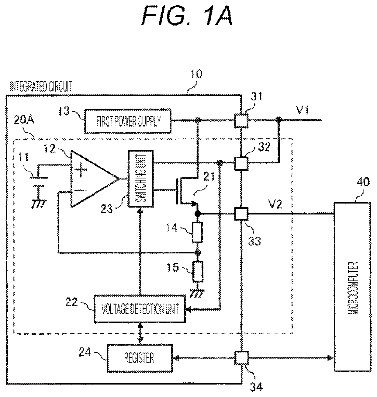
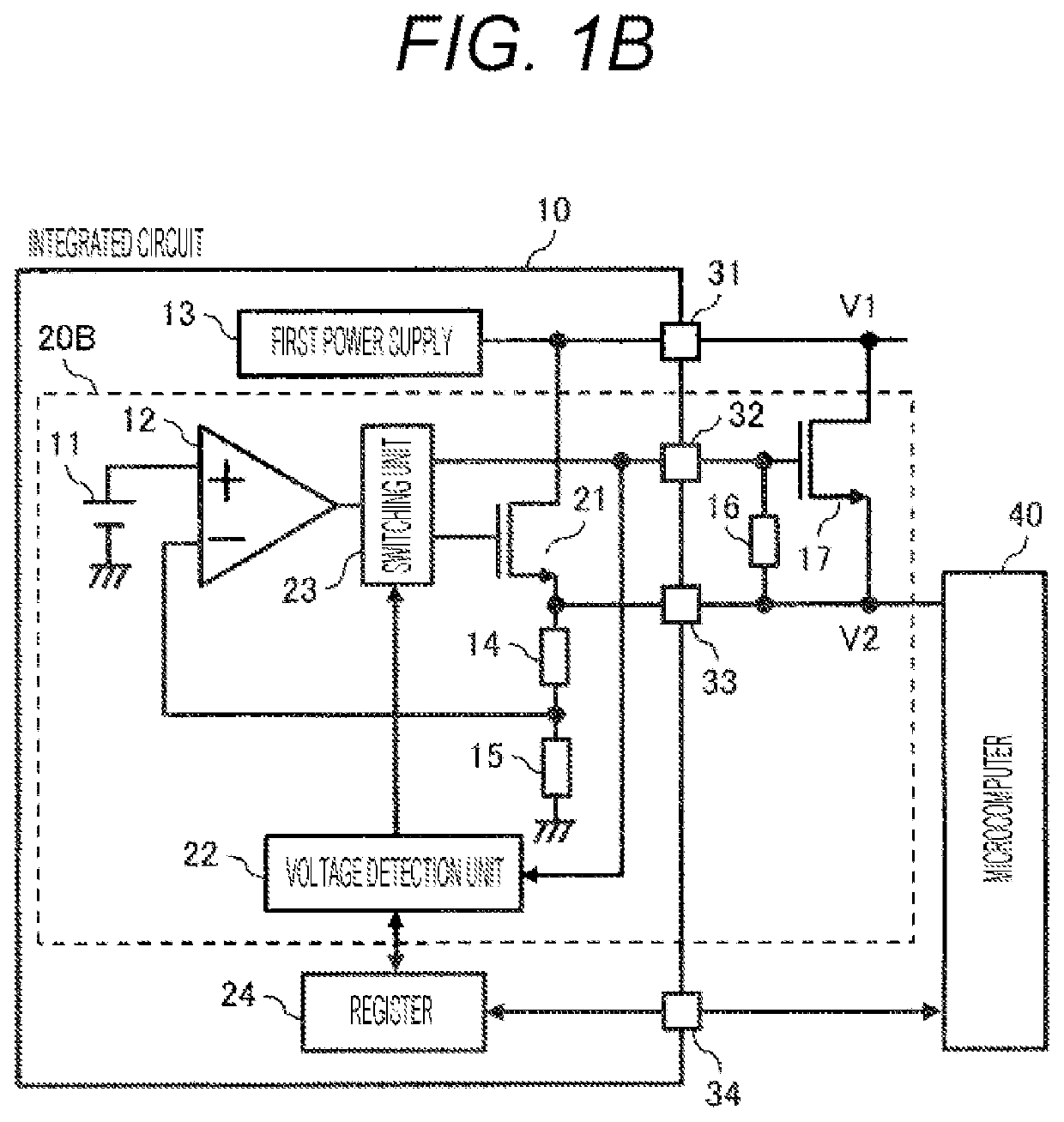
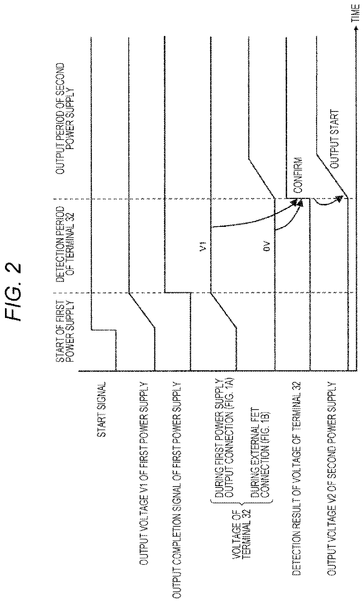
[0032]A first embodiment of the present invention will be described with reference to FIGS. 1A to 2. FIGS. 1A and 1B illustrate a circuit configuration diagram of a power supply device (power supply ASIC) of the present embodiment, and FIG. 2 is a timing chart illustrating an operation (action) of the present embodiment. FIG. 1A illustrates the power supply device at the time of driving a built-in FET (built-in NMOS FET) 21, and FIG. 1B illustrates the power supply device at the time of driving an external FET (external NMOS FET) 17.

[0033]The power supply device illustrated in FIGS. 1A and 1B includes an integrated circuit 10 and includes the external FET (external NMOS FET) 17 in FIG. 1B, and a microcomputer 40 as a load is connected to an output V2 of this power supply device.

[0034]The integrated circuit 10 includes a first power supply (circuit) 13 that outputs a voltage V1 via a terminal 31, a voltage detection unit 22 that detects a voltage of a terminal 32, a switching unit 23...

second embodiment

[0049]Hereinafter, a second embodiment of the present invention will be described with reference to FIGS. 3A to 4. FIGS. 3A and 3B illustrate a circuit configuration diagram of a power supply device (power supply ASIC) of the present embodiment, and FIG. 4 is a timing chart illustrating an operation (action) of the present embodiment.

[0050]In FIG. 3A, an output determination unit 25 that determines whether or not the output voltage V2 of the second power supply circuit 20A is normally output is added to the circuit configuration of FIG. 1A.

[0051]The output determination unit 25 determines whether the output voltage V2 of the second power supply circuit 20A is normally output at a start. If the output voltage V2 does not reach a desired (predetermined) voltage within a certain time, a connection of the switching unit 23 is reversed.

[0052]For example, when an open failure occurs in the terminal 32 in the circuit of FIG. 3A, a voltage of the terminal 32 is sometimes constant at 0 V as ...

third embodiment

[0057]Hereinafter, a third embodiment of the present invention will be described with reference to FIGS. 5A to 6. FIGS. 5A and 5B illustrate a circuit configuration diagram of a power supply device (power supply ASIC) of the present embodiment, and FIG. 6 is a timing chart illustrating an operation (action) of the present embodiment. The present embodiment is an example of a case where a PMOS FET is used as an FET.

[0058]FIG. 5A is obtained by changing the built-in NMOS FET 21 in FIG. 3A to a built-in PMOS FET 19, and FIG. 5B is obtained by changing the built-in NMOS FET 21 and the external NMOS FET 17 of FIG. 3B to the built-in PMOS FET 19 and an external PMOS FET 18. Further, the pull-down resistor 16 is changed to a pull-up resistor 36. When the external PMOS FET 18 is set as an output as in the present embodiment, a detected voltage of the terminal 32 is different from that in the case of the external NMOS FET 17 in the first and second embodiments. The pull-up resistor 36 is arr...


PUM


Abstract

Provided is a highly versatile and reliable power supply device (power supply ASIC) that can support electronic devices with a wide range of drive currents while suppressing a cost increase, and an electronic control device using the same. An electronic control device includes: a first power supply circuit that outputs a first voltage; a second power supply circuit that generates a second voltage from the first voltage; and a first MOSFET arranged independently of the first power supply circuit and the second power supply circuit. The second power supply circuit includes: a reference power supply that outputs a reference voltage; an amplifier that amplifies the reference voltage; a second MOSFET connected in parallel with the first MOSFET; a voltage detection unit that detects a voltage value of a gate terminal of the first MOSFET; and a switching unit that connects an output from the amplifier to either the gate terminal of the first MOSFET or a gate terminal of the second MOSFET. The switching unit is controlled based on a voltage value at a start detected by the voltage detection unit.

Description

TECHNICAL FIELD[0001]The present invention relates to a switching circuit of an output unit of a power supply device in an electronic control device, and particularly to a technology that is effective when applied to an in-vehicle electronic control device that requires control with a wide range of drive currents such as engine control and battery control.BACKGROUND ART[0002]A power supply device mounted on an electronic control device generally has a high current driving capability, and thus, can be used in a wide range of applications. Meanwhile, the use of the power supply device having the high current driving capability in applications for low current driving becomes over-qualified, which causes an increase in cost of the power supply device (electronic control device).[0003]Here, a semiconductor integrated circuit (IC) has realized high integration and low cost by integrating components in the IC, and a power supply device using the IC has been widely commercialized.[0004]In t...

Claims


Application Information

Patent Timeline
Patent Type & Authority Applications(United States)
IPC IPC(8): G05F1/565B60R16/033G05F1/595H03K17/22H03F3/68
CPCG05F1/565B60R16/033H03F3/68H03K17/223G05F1/595G05F1/59G05F1/465G05F1/577B60R16/03
Inventor DOI, MASAHIROOHARA, YURIYAMASHITA, TAKEO
Owner HITACHI ASTEMO LTD
Why Eureka
Try Eureka