Silicon precursor and method of fabricating silicon-containing thin film using the same

Pending Publication Date: 2021-11-11
HANSOL CHEM
View PDF1 Cites 0 Cited by
  • Summary
  • Abstract
  • Description
  • Claims
  • Application Information

AI Technical Summary

Benefits of technology

[0014]In particular, an object of the present disclosure is to provide a silicon precursor including a novel silicon compound which may ensure the behavior of ALD at high temperature due to its possible application at a high process temperature of 600° C. or higher, may form a silicon oxide film having a low impurity concentration

Problems solved by technology

Thus, a problem arises in that deposition of silicon-containing thin films using conventional precursors does not meet the required performance.
When a thin film is deposited on a highly integrated semiconductor device using a conventional precursor, a problem arises in that it is difficult to achieve excellent step coverage of the thin film and control the thickness thereof, and impurities are contained in the thin film.
However, since CVD and ALD have different reaction mechanisms, a pre

Method used


Image

  • Silicon precursor and method of fabricating silicon-containing thin film using the same
  • Silicon precursor and method of fabricating silicon-containing thin film using the same
  • Silicon precursor and method of fabricating silicon-containing thin film using the same

Examples


Example

EXAMPLE 1

Production of Diisopropylaminotrichlorosilane (C6H14Cl3NSi)

[0046]SiCl4 (1.0 eq.) was placed in a flask, diluted in pentane (12 eq.), and then cooled in a water bath maintained at 0° C. While the resulting solution was stirred, diisopropylamine (2.87 eq.) diluted in pentane (6 eq.) was added slowly to the solution. After completion of the addition, the mixture was stirred at room temperature for 15 hours. After completion of the reaction, the reaction mixture was filtered, and the filtrate solution was boiled at atmospheric pressure to remove the solvent. The obtained liquid was purified under reduced pressure to obtain a colorless transparent liquid.

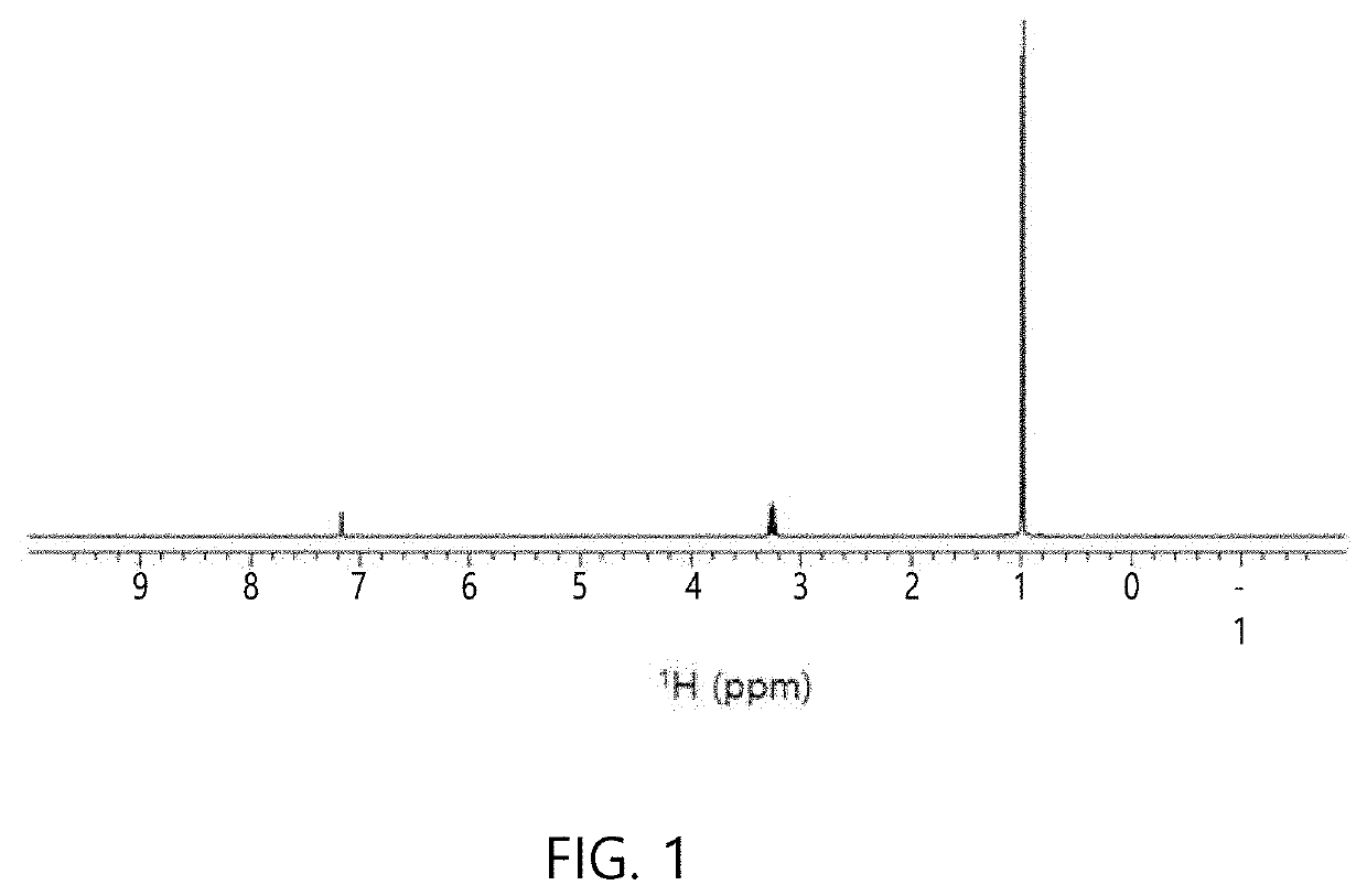
[0047]A reaction scheme for synthesis of diisopropylaminotrichlorosilane and the chemical structure of diisopropylaminotrichlorosilane are shown in the following Reaction Scheme and Chemical Structural Formula, and the chemical structure of diisopropylaminotrichlorosilane was verified by 1H-NMR as shown in FIG. 1.

[0048]In additi...

Example

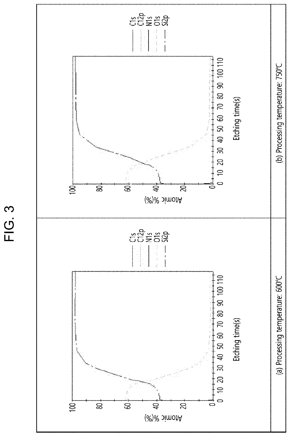
[0063][Experimental Example 1] Analysis of Composition of Silicon Oxide Film (SiO2) Fabricated from Precursor of Example 1

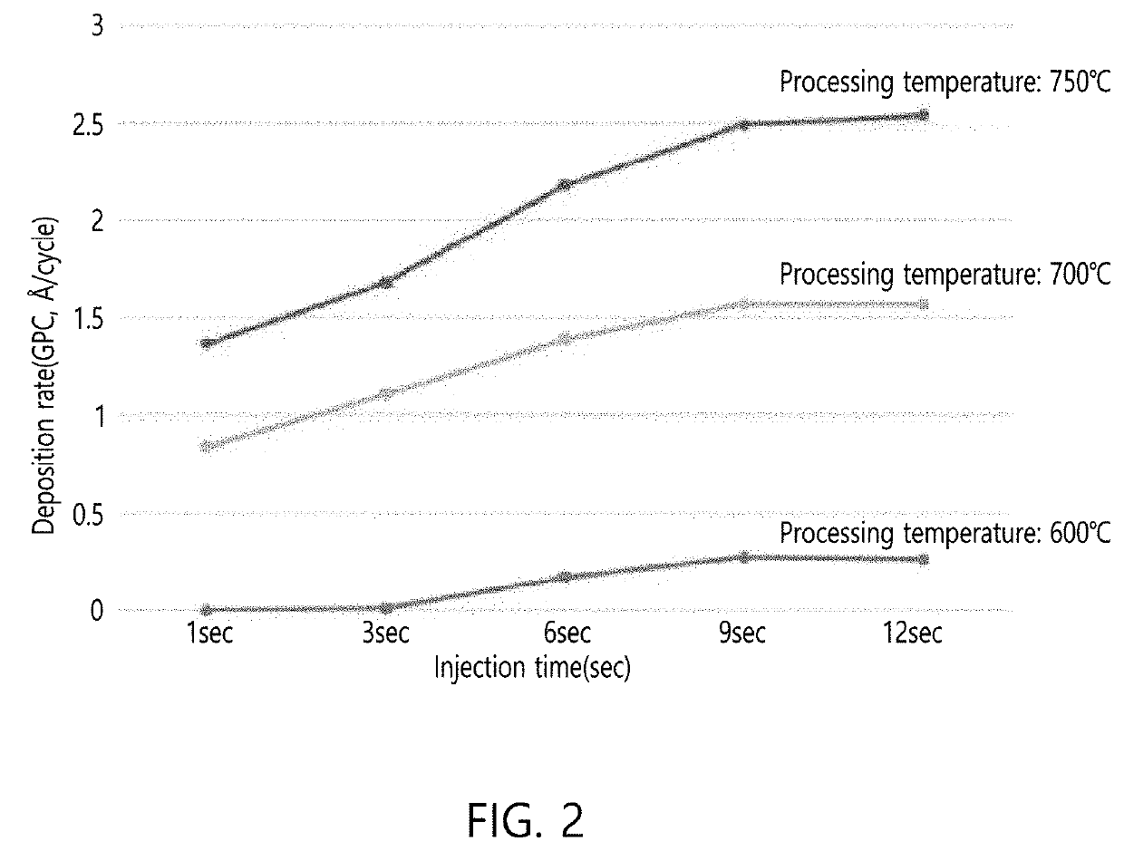
[0064]The compositions of the silicon oxide films fabricated by depositing the precursor of Example 1 and the mixture of oxygen and hydrogen (H2+O2) at process temperatures of 600° C. and 750° C., respectively, were analyzed by XPS analysis, and the results of the analysis are shown in FIG. 3.

[0065]As shown in FIG. 3, from the results of XPS analysis of all the thin films fabricated at process temperatures of 600° C. (FIG. 3a) and 750° C. (FIG. 3b), it could be confirmed that impurities such as carbon (C), chlorine (Cl) and nitrogen (N) were not detected, suggesting that the formed silicon thin films had excellent quality without containing impurities.

Example

[0066][Experimental Example 2] Surface Characteristics of Silicon Oxide Film (SiO2) Fabricated from Precursor of Example 1

[0067]The surface roughnesses (Ra) of the silicon oxide films fabricated by depositing the precursor of Example 1 and the mixture of oxygen and hydrogen (H2+O2) at process temperatures of 600° C. and 750° C., respectively, were measured by observation using atomic force microscopy (AFM) and scanning electron microscopy (SEM), and the results of the measurement are shown in FIG. 4.

[0068]As shown in FIG. 4, the surface roughnesses (Ra) were measured to range from 0.097 nm to 0.134 nm, indicating that the silicon oxide films all had low roughness (1.5 Å or less). In addition, it could be confirmed that the roughness increased as the process temperature increased (FIG. 4a (process temperature: 600° C., and Ra: 0.097 nm) and FIG. 4b (process temperature: 750° C., and Ra: 0.134 nm)).

[0069]This low surface roughness could also be confirmed by SEM.


PUM

PropertyMeasurementUnit
Temperatureaaaaaaaaaa
Densityaaaaaaaaaa
Surface roughnessaaaaaaaaaa

Abstract

The present disclosure relates to a vapor deposition compound which may be deposited as a thin film by vapor deposition, and specifically, to a silicon precursor which is applicable to atomic layer deposition (ALD) or chemical vapor deposition (CVD) and may be deposited at high rate, particularly by high-temperature ALD, and a method for fabricating a silicon-containing thin film using the same.

Description

CROSS-REFERENCE TO RELATED APPLICATION[0001]This application claims priority from and the benefit of Korean Patent Application No. 10-2020-0054948, filed on May 8, 2020, which is hereby incorporated by reference for all purposes as if set forth herein.BACKGROUNDField[0002]The present disclosure relates to a vapor deposition compound which may be deposited as a thin film by vapor deposition, and more particularly, to a novel silicon precursor which is applicable to atomic layer deposition (ALD) or chemical vapor deposition (CVD) and may be used for the fabrication of a thin film having excellent quality, particularly at a high process temperature, and a method for fabricating a silicon-containing thin film using the same.Discussion of the Background[0003]Silicon-containing thin films are used as semiconductor substrates, diffusion masks, oxidation barriers and dielectric films in semiconductor technologies such as microelectronic devices including RAMs (memory and logic chips), flat ...

Claims


Application Information

Patent Timeline
IPC IPC(8): C09D183/16C23C16/455C23C16/50
CPCC09D183/16C23C16/50C23C16/45553C23C16/402C23C16/448C07F7/10C09D183/08C08G77/26C23C16/401C23C16/345C23C16/30H01L21/02214H01L21/02219H01L21/02271
Inventor AN, JAE-SEOKKIM, YEONG-EUNSEOK, JANG-HYUNPARK, JUNG-WOO
Owner HANSOL CHEM
Why Eureka
Try Eureka