Aluminum nitride substrate and group-III nitride laminate

a technology of aluminum nitride and nitride, which is applied in the direction of crystal growth process, semiconductor laser, polycrystalline material growth, etc., can solve the problem that the conventional art cannot be applied, and achieve the effect of improving the growth surface of the group iii nitride single crystal layer, low impurity concentration, and high quality light emitting device elements

Active Publication Date: 2016-05-17
TOKUYAMA CORP
View PDF27 Cites 1 Cited by
  • Summary
  • Abstract
  • Description
  • Claims
  • Application Information

AI Technical Summary

Benefits of technology

[0029]By using the aluminum nitride substrate of the present invention as the substrate for the crystal growth of the group III nitride single crystal layer, the flatness of the growth surface of the group III nitride single crystal layer can be improved. Also, the composition distribution of the group III nitride single crystal layer can be further uniform, and the impurity concentration can be made low. As a result, a high quality light emitting device element can be produced. Among these, the aluminum nitride substrate of the present invention exhibits particularly excellent effect in case of growing AlGaInBN layer which satisfies the composition of Al1−(x+y+z)GaxInyBzN which has close lattice constant (note that, x, y, and z are independently a rational number of 0 or more and less than 0.5 respectively, and a sum of x, y, and z is less than 0.5) thereon. Therefore, the group III nitride layered product comprising aluminum nitride substrate of the present invention can be used as the deep ultraviolet light emitting element.

Problems solved by technology

That is, in case of growing the mixed crystal layer made of the group III nitride single crystal having 50 atom % or more of Al composition, the conventional art cannot be applied for improving the flatness of mixed crystal layer, and to have uniform composition distribution or to reduce the impurity concentration.

Method used


Image

  • Aluminum nitride substrate and group-III nitride laminate
  • Aluminum nitride substrate and group-III nitride laminate

Examples


example 1

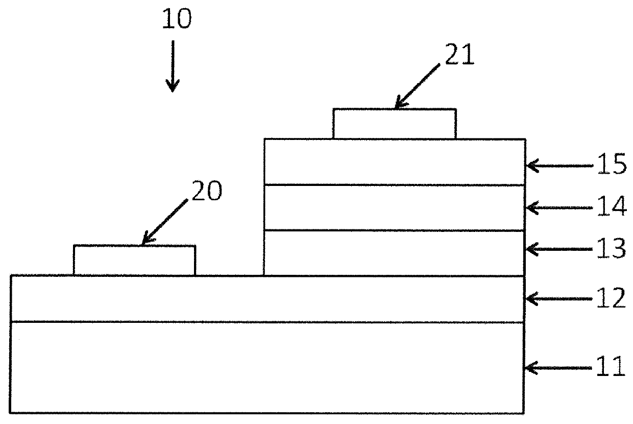
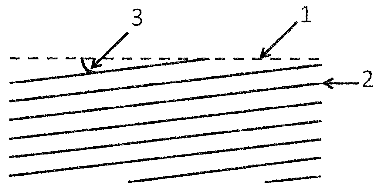
[0078]The surface and the backside of the c-plane aluminum nitride substrate made of aluminum nitride single crystal having the thickness of about 500 μm was ground, and CMP polishing was carried out. Thereby, the aluminum nitride substrate (the aluminum nitride substrate consisting only of the AlN single crystal layer) having the thickness of 200 μm wherein the principal plane of the aluminum nitride substrate comprises the plane inclined to “m” axis direction at 0.11° from (0001) plane of a wurzite structure was obtained. The radius of the curvature of this aluminum nitride substrate was 20 m, and the surface roughness (Ra) was 0.17 nm. Also, the inclination to “a” axis direction from (0001) plane of a wurzite structure was 0.00°.

[0079]On this aluminum nitride substrate, 1 μm of “n” layer (Al0.7Ga0.3N) doped with Si was formed by MOCVD method. Then, the barrier layer and the well layer were formed on said “n” layer by MOCVD method so that the quantum well layer has the following s...

example 2

[0081]The same procedure and the evaluation were carried out as the example 1; except that the aluminum nitride substrate wherein the principal plane has the plane inclined to “m” axis direction at 0.23° from (0001) plane of a wurzite structure was used. For the physical properties (the crystalline quality, the radius of the curvature, the surface roughness (Ra), the thickness, and the inclination to “a” direction) of the principal plane except for the off angle of the principal plane, those as same as the aluminum nitride substrate used in example 1 was used.

[0082]As a result of the PL measurement of the obtained substrate (the group III nitride layered product) of after the growth of the “n” layer and the quantum well layer, the peak position of the luminescence peak derived from the quantum well layer was 4.86 eV, and its FWHM was 203 meV. The surface roughness (Ra) was 0.20 nm. The results are shown in Table 1.

example 3

[0083]The same procedure and the evaluation were carried out as the example 1; except that the aluminum nitride substrate wherein the principal plane has the plane inclined to “m” axis direction at 0.32° from (0001) plane of a wurzite structure was used. For the physical properties (the crystalline quality, the radius of the curvature, the surface roughness (Ra), the thickness, and the inclination to “a” direction) of the principal plane except for the off angle of the principal plane, those as same as the aluminum nitride substrate used in example 1 was used.

[0084]As a result of the PL measurement of the obtained substrate (the group III nitride layered product) of after the growth of the “n” layer and the quantum well layer, the peak position of the luminescence peak derived from the quantum well layer was 4.79 eV, and its FWHM was 208 meV. The surface roughness (Ra) was 0.30 nm. The results are shown in Table 1.


PUM

PropertyMeasurementUnit
band gapaaaaaaaaaa
band gapaaaaaaaaaa
off angleaaaaaaaaaa

Abstract

A substrate includes aluminum nitride, wherein the aluminum nitride substrate has on at least a surface thereof an aluminum nitride single-crystal layer having as a principal plane a plane that is inclined 0.05° to 0.40° in the m-axis direction from the (0001) plane of a wurzite structure.

Description

[0001]This application is a U.S. national stage application of PCT / JP2013 / 073806 filed on 4 Sep. 2013, and claims priority to Japanese patent document 2012-199685 filed on 11 Sep. 2012, the entireties of which are incorporated herein by reference.TECHNICAL FIELD[0002]The present invention relates to a novel aluminum nitride substrate. Specifically, the present invention relates to the novel aluminum nitride substrate comprising an aluminum nitride single crystal layer having an plane inclined in a particular direction as a principal plane.DESCRIPTION OF THE RELATED ART[0003]The aluminum nitride has a wide forbidden band gap of 6.2 eV and is a semiconductor with direct band gap. Therefore, a mixed crystal of group III nitride semiconductors such as aluminum nitride, a gallium nitride (GaN) and indium nitride (InN), particularly the mixed crystal having 50 atom % or more of Al composition in group III nitride semiconductors (hereinafter, it may be referred as “Al based group III nitri...

Claims


Application Information

Patent Timeline
Patent Type & Authority Patents(United States)
IPC IPC(8): H01L29/04B82Y20/00C30B29/68H01L29/20H01L33/16C30B25/18C30B29/40H01L21/02H01S5/343H01S5/02H01S5/32H01L33/32H01L33/02
CPCC30B25/186C30B29/403C30B29/68B82Y20/00H01L29/045H01L29/2003H01L33/16H01S5/343H01S5/0206H01S5/3202H01S5/34333H01L21/02389H01L21/02433H01L21/0254H01L21/0262H01L33/02H01L33/32
Inventor HIRONAKA, KEIICHIROKINOSHITA, TORU
Owner TOKUYAMA CORP
Why Eureka
Try Eureka