Semiconductor device for high voltage isolation

a high-voltage isolation, semiconductor technology, applied in semiconductor devices, electronic switching, pulse techniques, etc., can solve the problems of high reverse breakdown voltage of diodes, complex eternal circuitry, unsuitable, etc., and achieve the effect of low impurity concentration and high impurity concentration

Active Publication Date: 2020-01-23
MOSWAY TECH LTD
View PDF1 Cites 0 Cited by
  • Summary
  • Abstract
  • Description
  • Claims
  • Application Information

AI Technical Summary

Benefits of technology

[0005]In accordance with a first aspect of the invention, there is provided a semiconductor device, comprising: a substrate of a first conductivity type with relatively low impurity concentration; a first region of a second conductivity type with relatively low impurity concentration arranged on the substrate; a second region of the first conductivity type with relatively high impurity concentration, arranged on the substrate; first and second conductors, arranged on the first region and separated by an isolator layer; and a third conductor, separated from the first and second conductors by the isolator layer, arranged on the second region; wherein the first conductor is arranged to provide a drain terminal, the second conductor is arranged to provide a source terminal, the third conductor is arranged to provide a gate terminal. Preferably, the first conductivity type is P-type and the second conductivity type is N-type. The semiconductor device is preferably a JFET device, in particular, a high voltage JFET device.

Problems solved by technology

Such integration requires a diode with high reverse breakdown voltage that is normally not available in typical integrated circuit process technology platforms.
But the use of a high voltage LDMOS device usually requires complex eternal circuitry, which is not desirable.

Method used


Image

  • Semiconductor device for high voltage isolation
  • Semiconductor device for high voltage isolation
  • Semiconductor device for high voltage isolation

Examples


Embodiment Construction

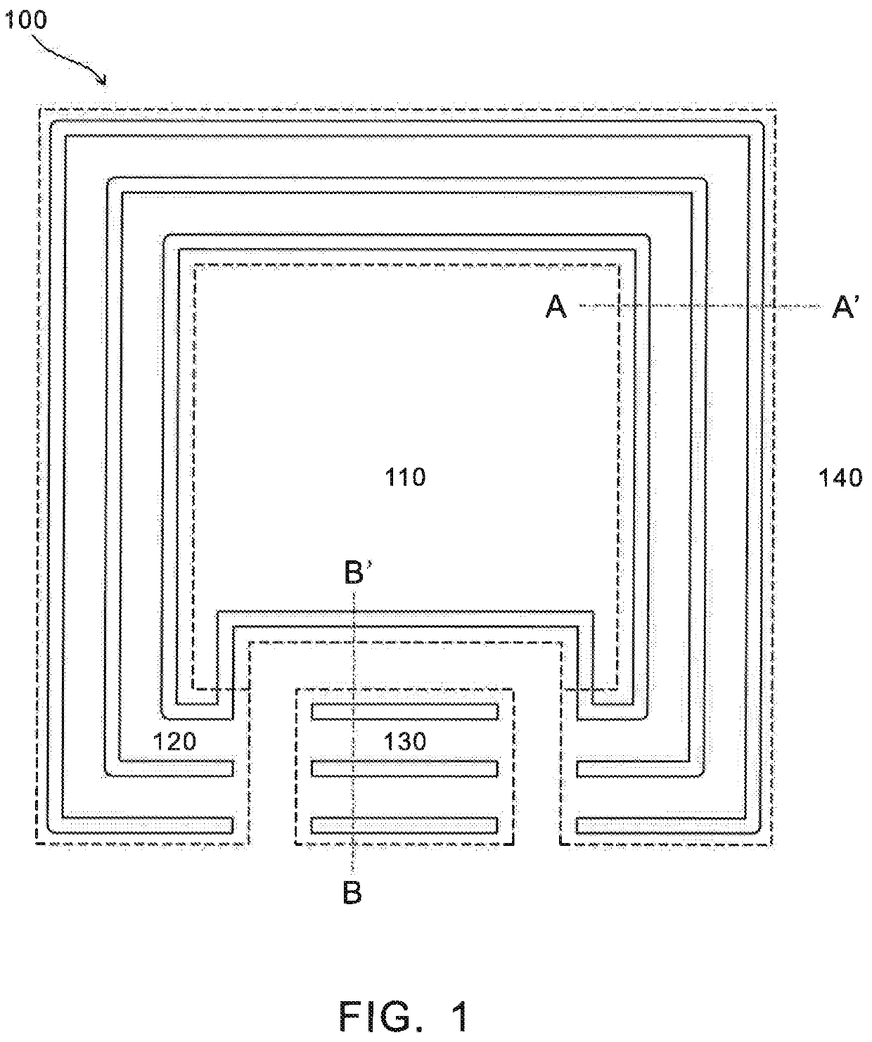
[0035]FIG. 1 is the topology of a semiconductor device 100 in one embodiment of the invention. In this embodiment, the semiconductor device 100 includes two high voltage JFET devices. The semiconductor device 100 is arranged to isolate a floating high voltage region 110, such as one in a half bridge driver (not shown), from a low / medium voltage region 140. Regions 120, 130 are N-channel regions between the drain and source of the high voltage JFET device.

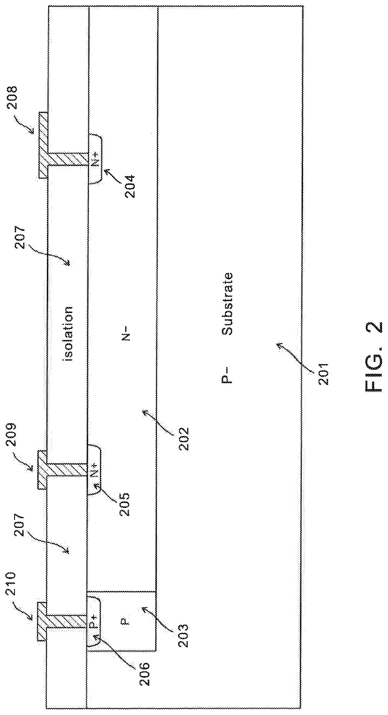
[0036]FIG. 2 shows the sectional view A-A′ of the semiconductor device of FIG. 1. As shown in FIG. 2, the device includes a base P-substrate layer 201. A P diffusion region 203 is arranged on the P-substrate layer 201. A N-region 202 is arranged on the P-substrate layer 201, adjacent the P diffusion region 203. A P+diffusion region 206 is arranged on the P diffusion region 203. A conductor 210 arranged to provide a gate terminal is arranged on and connected to the P+ diffusion region 206. Two separate N+ diffusion regions 204, 205, ...


PUM

PropertyMeasurementUnit
conductivityaaaaaaaaaa
concentrationaaaaaaaaaa
electrical currentaaaaaaaaaa

Abstract

A semiconductor device includes a substrate of a first conductivity type with relatively low impurity concentration; a first region of a second conductivity type with relatively low impurity concentration, =located in the substrate; a second region of the first conductivity type with relatively high impurity concentration, located in the substrate; first and second conductors, located on the first region and separated from each other by an isolator layer; and a third conductor, separated from the first and second conductors by the isolator layer, and located on the second region. The first conductor provides a drain terminal. The second conductor provides a source terminal. The third conductor provides a gate terminal.

Description

TECHNICAL FIELD[0001]The invention relates to a semiconductor device and particularly, although not exclusively, to a semiconductor device arranged to provide high voltage isolation.BACKGROUND[0002]Conventional high voltage half bridge driver integrated circuit may include a built-in bootstrap diode arranged between the low side supply voltage node VCC and the bootstrap supply voltage node VB, for connection with a bootstrap capacitor (not shown). During normal operation, energy is transferred from the low side power supply with nodes VCC and GND to high side supply decoupling capacitor between nodes VB and VS, via the bootstrap diode. However, in some applications it is preferable to integrate the bootstrap diode in the half-bridge driver integrated circuit for simplifying the application circuit. Such integration requires a diode with high reverse breakdown voltage that is normally not available in typical integrated circuit process technology platforms.[0003]One solution is to us...

Claims


Application Information

Patent Timeline
Patent Type & Authority Applications(United States)
IPC IPC(8): H01L29/06H01L29/861H03K17/687
CPCH01L29/0623H01L29/861H03K17/6871H01L27/085H01L27/098H01L29/0692H01L29/0696H01L29/1075H01L29/808
Inventor TANG, CHI KEUNGCHAN, PETER ON BON
Owner MOSWAY TECH LTD
Why Eureka
Try Eureka