High-voltage pulse generator, gas laser apparatus, and method for manufacturing electronic device
Pending Publication Date: 2021-11-25
NAT UNIV CORP NAGAOKA UNIV TECH +1
View PDF0 Cites 0 Cited by
Summary
Abstract
Description
Claims
Application Information
AI Technical Summary
This helps you quickly interpret patents by identifying the three key elements:
Problems solved by technology
Method used
Benefits of technology
Benefits of technology
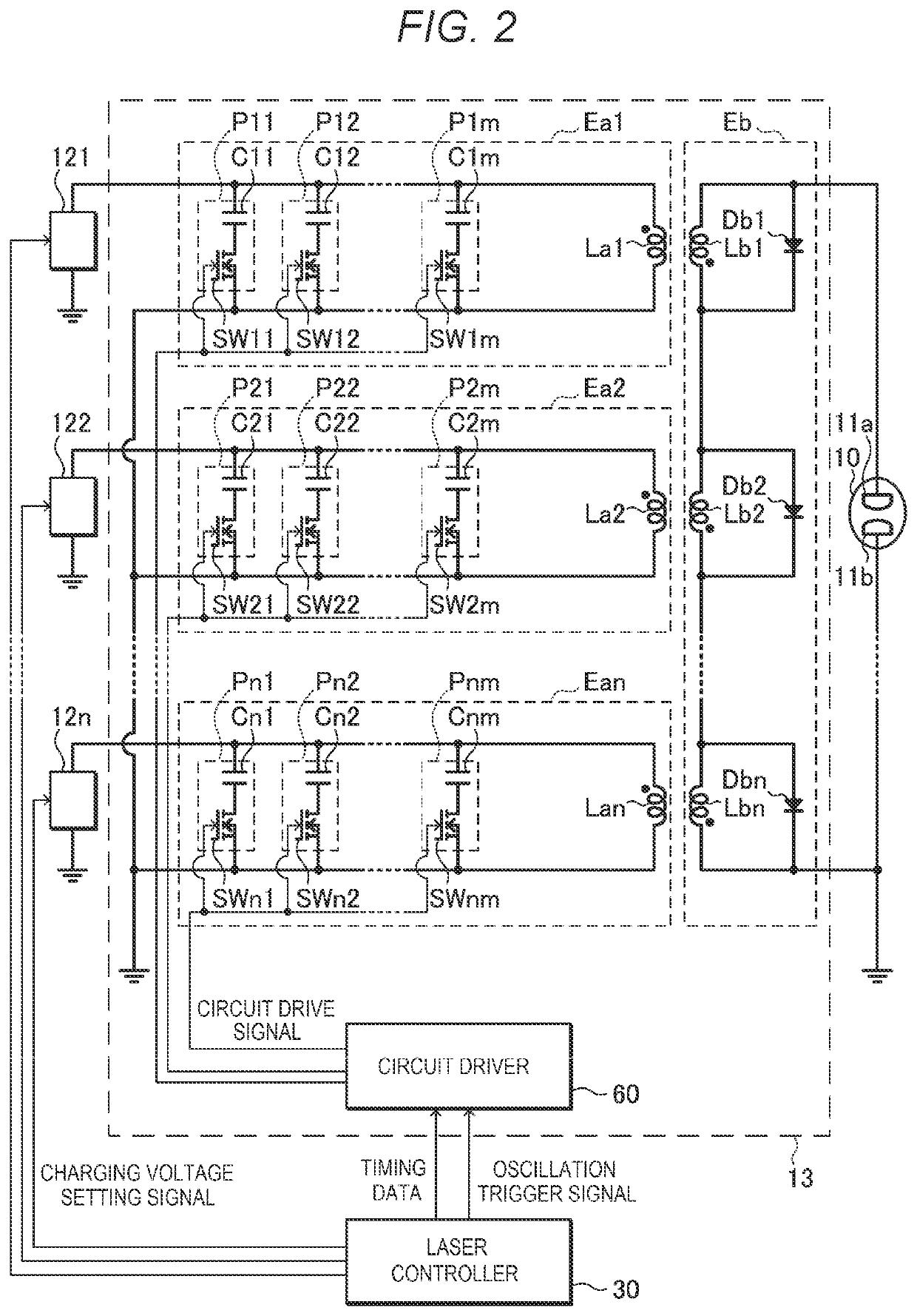
[0007]A high-voltage pulse generation device according to a viewpoint of the present disclosure is a high-voltage pulse generation device configured to apply a pulsed high voltage to a space between a pair of discharge electrodes disposed in a laser chamber of a gas laser apparatus, the high-voltage pulse generation device including n transformer cores that form a transformer, where n is a natural number greater than or equal to two, n primary electric circuits of the transformer, the n primary electric circuits each having a first terminal connected to a reference potential and a second terminal connected to a charger, the n primary electric circuits each including one or more primary coils, one or more diodes connected in parallel to the one or more primary coils, and one or more pulse generators connected in parallel to the one or more primary coils, and a secondary electric circuit of the transformer, the secondary electric circuit including a secondary coil and connected to the pair of discharge electrodes.
[0008]A gas laser apparatus according to another viewpoint of the present disclosure is a gas laser apparatus including a laser chamber, a pair of discharge electrodes disposed in the laser chamber, and a high-voltage pulse generation device configured to apply a pulsed high voltage to a space between the pair of discharge electrodes. The high-voltage pulse generation device is a high-voltage pulse generation device configured to apply the pulsed high voltage to the space between the pair of discharge electrodes disposed in the laser chamber of the gas laser apparatus, the high-voltage pulse generation device including n transformer cores that form a transformer, where n is a natural number greater than or equal to two, n primary electric circuits of the transformer, the n primary electric circuits each having a first terminal connected to a reference potential and a second terminal connected to a charger, the n primary electric circuits each incl
Problems solved by technology
Since KrF and ArF excimer laser apparatuses each have a wide spectral linewidth ranging from about 350 to 400 pm in spontaneous oscillation, the chromatic aberrations occur in associatio
Method used
Image
Click on the blue label to locate the original text in one second.
Reading with bidirectional positioning of images and text.
Examples
Example
[0153]According to the first embodiment, the diode Dai is disposed in the primary electric circuit Eai, whereby the secondary electric circuit Eb can be simplified. The output inductance of the pulse power module 13 can thus be reduced.
[0154]Furthermore, for example, when the primary electric circuit Ea1 is not driven and the remaining n−1 primary electric circuits Ea2 to Ean are driven, damage to the switches SW11 to SWim and the charger 12 can be suppressed.
[0155]Moreover, since the current flows into the diode Dai when the capacitor Cij is charged, the capacitor Cij can be efficiently charged. In addition, since the flow of current in the primary coil Lai can be suppressed during the charging process, generation of a magnetic flux in the transformer core TCi can be suppressed, whereby energy loss can be suppressed.
[0156]The other points in the first embodiment are the same as those in Comparable Example described above.
3. Pulse Power Module Mounted on Circular Substrate
Example
[0157]FIG. 8A is a plan view showing a second embodiment in which the pulse power module 13 is mounted on a circular substrate. FIG. 8B diagrammatically shows the cross section taken along the line VIIIB-A-VIIIB in FIG. 8A. It is, however, noted that FIG. 8B is not a cross-sectional view of the secondary coil Lb but is a side view thereof. FIGS. 8A and 8B show one primary electric circuit Eai out of the n primary electric circuits Ea1 to Ean, one transformer core TCi, and part of the secondary coil Lb.
[0158]The transformer core TCi has an annular shape. A magnetic circuit MC is formed along the annular shape that forms the transformer core TCi, as shown in FIG. 8A. The transformer core TCi is located in a first plane PLi, as shown in FIG. 8B. The first plane PLi is parallel to a plane HZ. The magnetic circuit MC is formed along the first plane PLi.
[0159]The secondary coil Lb is formed of a conductive member having a cylindrical shape. The secondary coil Lb has a through hole TH, as ...
Example
[0189]The other points in the third embodiment are the same as those in the second embodiment.
5. Pulse Power Module Disposed in Laser Chamber
PUM
Abstract
A high-voltage pulse generation device configured to apply a pulsed high voltage to the space between a pair of discharge electrodes disposed in a laser chamber of a gas laser apparatus includes n transformer cores that form a transformer, where n is a natural number greater than or equal to two, n primary electric circuits of the transformer, the n primary electric circuits each having a first terminal connected to a reference potential and a second terminal connected to a charger, the n primary electric circuits each including one or more primary coils, one or more diodes connected in parallel to the one or more primary coils, and one or more pulse generators connected in parallel to the one or more primary coils, and a secondary electric circuit of the transformer, the secondary electric circuit including a secondary coil and connected to the pair of discharge electrodes.
Description
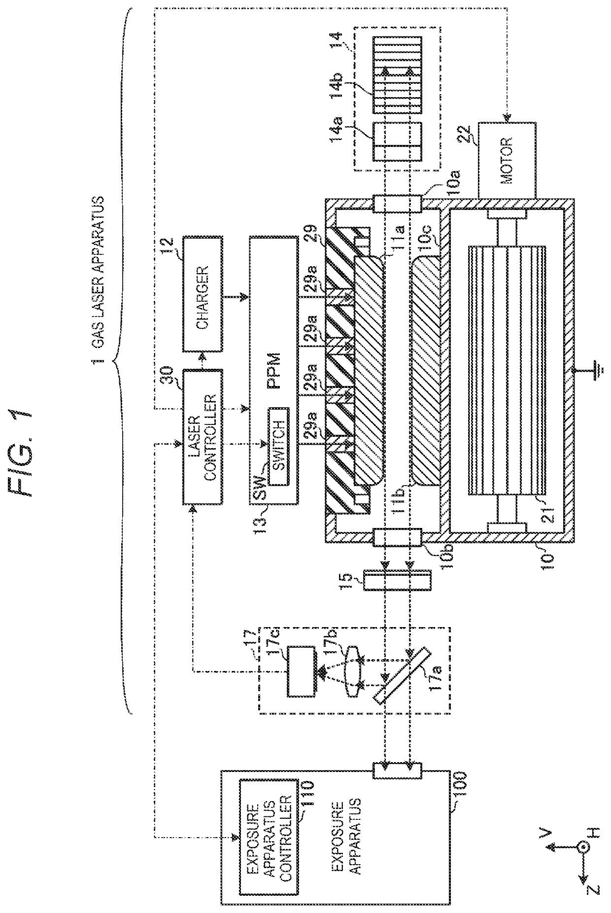
CROSS-REFERENCE TO RELATED APPLICATIONS[0001]The present application is a continuation application of International Application No. PCT / JP2019 / 012902, filed on Mar. 26, 2019, the entire contents of which are hereby incorporated by reference.BACKGROUND1. Technical Field[0002]The present disclosure relates to a high-voltage pulse generation device, a gas laser apparatus, and a method for manufacturing an electronic device.2. Related Art[0003]A semiconductor exposure apparatus is required to improve the resolution thereof as a semiconductor integrated circuit is increasingly miniaturized and highly integrated. The semiconductor exposure apparatus is hereinafter referred simply to as an “exposure apparatus”. To improve the resolution, reduction in the wavelength of light output from a light source for exposure is underway. A gas laser apparatus is used as the light source for exposure in place of a mercury lamp in related art. At present, a KrF excimer laser apparatus, which is configur...
Claims
Application Information
Patent Timeline
Application Date:The date an application was filed.
Publication Date:The date a patent or application was officially published.
First Publication Date:The earliest publication date of a patent with the same application number.
Issue Date:Publication date of the patent grant document.
PCT Entry Date:The Entry date of PCT National Phase.
Estimated Expiry Date:The statutory expiry date of a patent right according to the Patent Law, and it is the longest term of protection that the patent right can achieve without the termination of the patent right due to other reasons(Term extension factor has been taken into account ).
Invalid Date:Actual expiry date is based on effective date or publication date of legal transaction data of invalid patent.

