Unlock instant, AI-driven research and patent intelligence for your innovation.

Touch structure, manufacturing method thereof, and display device

a manufacturing method and touch technology, applied in the field of display technologies, can solve the problems of material cracking, poor mechanical reliability of flexible or foldable panels, and obstacles to the mass production of such products, and achieve the effects of improving the overall flexibility and bending resistance of metal mesh, improving structure, and improving mechanical reliability

Inactive Publication Date: 2021-12-02
WUHAN CHINA STAR OPTOELECTRONICS SEMICON DISPLAY TECH CO LTD
View PDF0 Cites 0 Cited by
  • Summary
  • Abstract
  • Description
  • Claims
  • Application Information

AI Technical Summary

Benefits of technology

The invention is a new method of making a touch structure for flexible displays. It involves creating grooves in an insulating layer to create a buffer angle with the layer, which results in a curved shape of the metal mesh. This makes the mesh more flexible and reduces stress between the metal meshes, which prevents failure issues under repeated bending and impact. The method is simple and can be used in industrial production. The overall effect of this invention is to improve the flexibility and bending resistance of metal mesh, making flexible devices easier to bend and better structured.

Problems solved by technology

However, poor mechanical reliability of flexible panels with flexible or foldable features is a major obstacle to the mass production of such products.
After multiple continuous bendings, material will crack and accelerate the failure of the products, especially occurs in a display touch layer.
After multiple bendings, a touch circuit is destroyed to lose a touch function.
However, an intersection of the mesh and an included angle of the metal will affect strength of an overall flexible touch system.

Method used


Image

  • Touch structure, manufacturing method thereof, and display device
  • Touch structure, manufacturing method thereof, and display device
  • Touch structure, manufacturing method thereof, and display device

Examples


Embodiment Construction

[0034]The following embodiments are described with reference to the accompanying drawings to illustrate specific embodiments in which the present invention can be implemented. The directional terms mentioned in the present invention, such as “up”, “down”, “front”, “rear”, “left”, “right”, “top”, “bottom”, etc., are only for reference to a direction of the accompanying drawings direction. Therefore, the directional terms used are for explaining and understanding the present invention, but not for limiting the present invention.

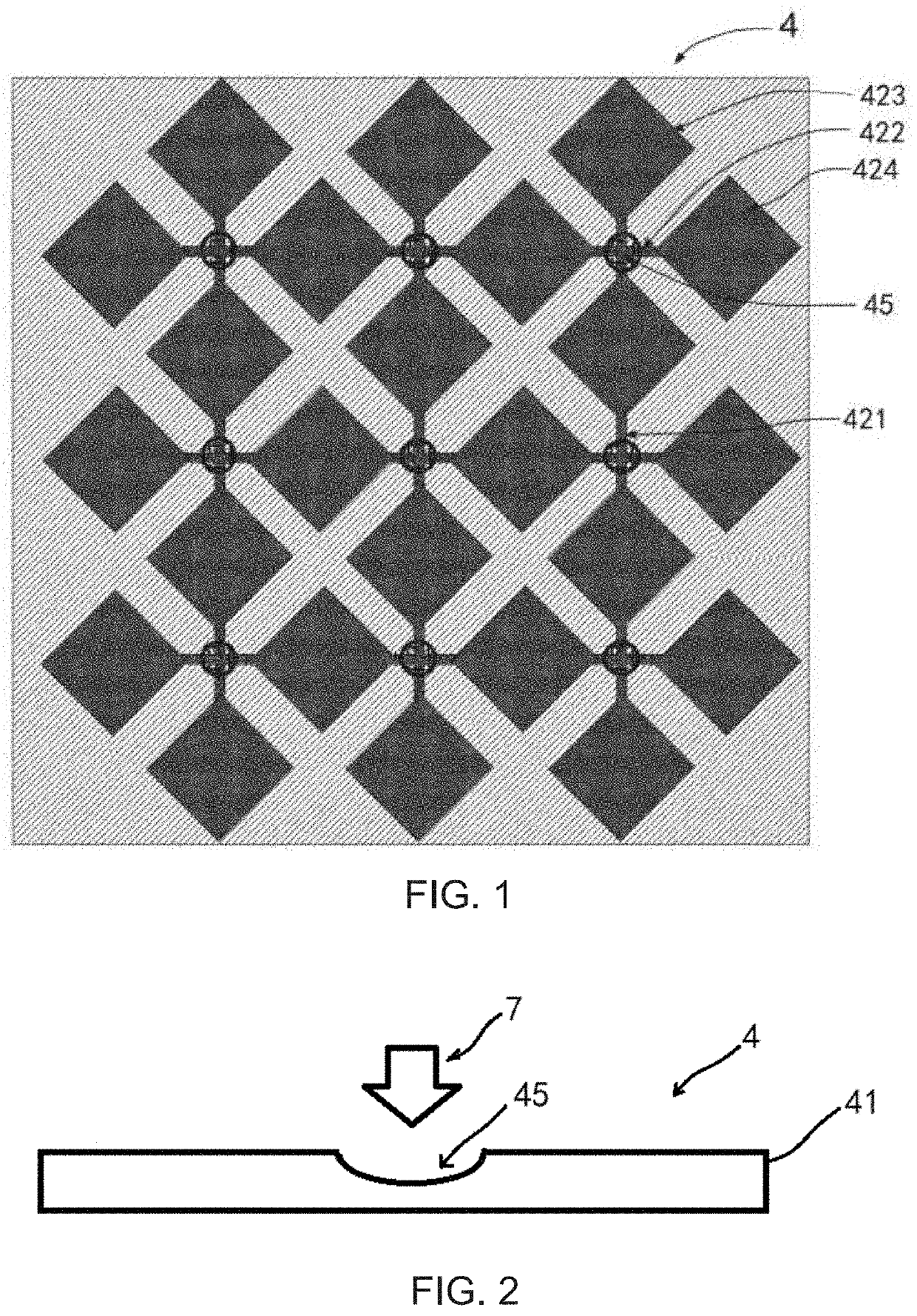
[0035]As shown in FIG. 6, in one embodiment, a touch structure 4 of the present invention includes an insulating layer 41, a metal mesh 42, an insulating filling layer 43, and a protective layer 44.

[0036]As shown in FIG. 2, one surface of the insulating layer 41 defines a plurality of grooves 45. Only one of the grooves 45 is shown in the figure to clearly show an enlarged structure of the groove 45. In this embodiment, the insulating layer 41 is a flexible ino...


PUM


Abstract

Disclosed are a touch structure, a manufacturing method thereof, and a display device. The touch structure includes an insulating layer defining a plurality of grooves on one surface of the insulating layer; a metal mesh having a plurality of first traces arranged in parallel to each other and a plurality of second traces arranged in parallel to each other, wherein the first traces and the second traces are intersected, the metal mesh is disposed on the surface of the insulation layer defining the grooves, the grooves are defined at an intersection of the first traces and the second traces, the first traces are disposed inside the grooves, and the second traces are disposed above the grooves; and an insulating filling layer filled in the grooves and configured to insulatingly separate the first traces and the second traces.

Description

FIELD OF INVENTION[0001]The present disclosure relates to the field of display technologies, and more particularly to a touch structure, a manufacturing method thereof, and a display device.BACKGROUND OF INVENTION[0002]With the rapid development of display technologies in recent years, active matrix organic light emitting diode (AMOLED) flexible displays have attracted much attention. Bendable, and even foldable, fixed curved mobile phones having large-size full-screens will be widely used in the future market. However, poor mechanical reliability of flexible panels with flexible or foldable features is a major obstacle to the mass production of such products. After multiple continuous bendings, material will crack and accelerate the failure of the products, especially occurs in a display touch layer. After multiple bendings, a touch circuit is destroyed to lose a touch function.[0003]Metal mesh technology uses metal materials such as silver and copper to grow on glass or plastic fi...

Claims


Application Information

Patent Timeline
IPC IPC(8): G06F3/041H01L27/32
CPCG06F3/0412G06F2203/04102G06F2203/04103H01L27/323G06F3/041G06F3/0446G06F2203/04112H10K59/40
Inventor XIE, MING
Owner WUHAN CHINA STAR OPTOELECTRONICS SEMICON DISPLAY TECH CO LTD