Flash memory device and bit line charging method thereof
- Summary
- Abstract
- Description
- Claims
- Application Information
AI Technical Summary
Benefits of technology
Problems solved by technology
Method used
Image
Examples
Embodiment Construction
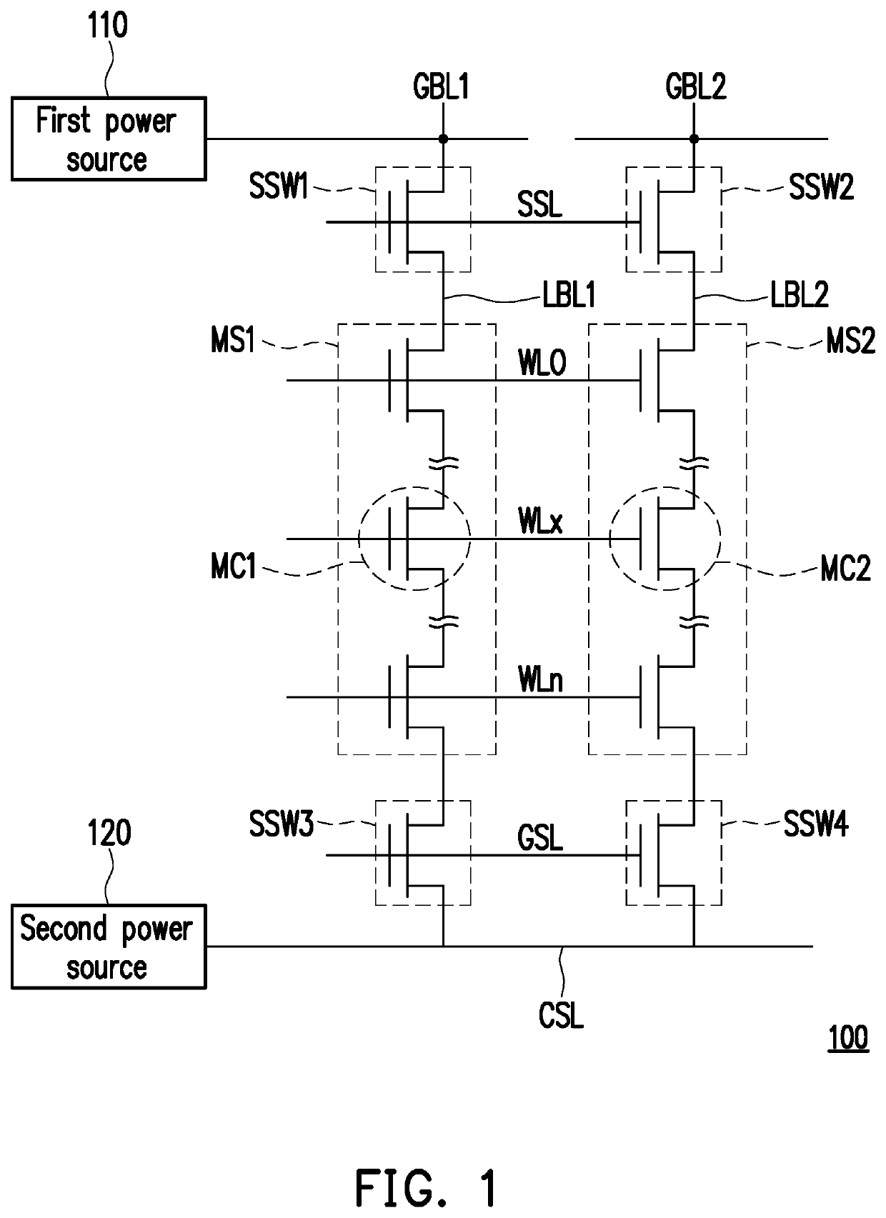
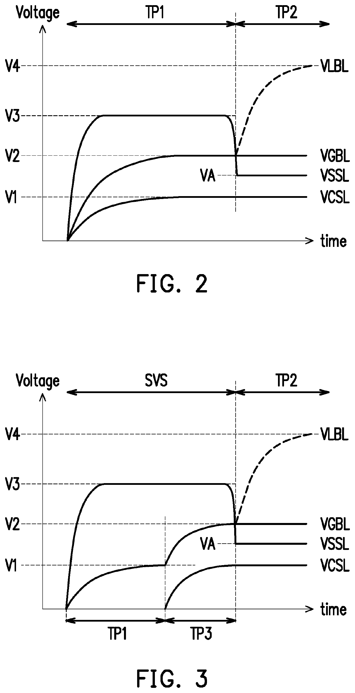
[0014]Please refer to FIG. 1, which is a circuit diagram of a flash memory device according to an embodiment of present disclosure. The flash memory device 100 includes memory strings MS1 and MS2, selection switches SSW1 and SSW2, a first power source 110 and a second power source 120. Each of the memory strings MS1 and MS2 has a plurality of memory cells, and the memory cells are respectively coupled to a plurality of word lines WL0˜WLn. The memory string MS1 is coupled to a local bit line LBL1 and the memory string MS2 is coupled to a local bit line LBL2. The selection switch SSW1 is coupled between a global bit line GBL1 and the local bit line LBL1, and the selection switch SSW2 is coupled between the global bit line GBL2 and the local bit line LBL2. The selection switches SSW1 and SSW2 receive a selection signal SSL, and are turned on or turned-off according to the selection signal SSL. Besides, the memory string MS1 is coupled to a source line CSL through a switch SSW3, and the...
PUM
 Abstract
Description
Claims
Application Information


