Semiconductor light emitting device

a technology of light-emitting devices and semiconductors, which is applied in the direction of semiconductor devices, basic electric elements, electrical appliances, etc., can solve the problems of insufficient airtightness and more easily deteriorated structures, and achieve the effects of improving scalability, high airtightness, and easy deterioration

Pending Publication Date: 2021-12-09
STANLEY ELECTRIC CO LTD
View PDF0 Cites 2 Cited by
  • Summary
  • Abstract
  • Description
  • Claims
  • Application Information

AI Technical Summary

Benefits of technology

[0005]However, a further improvement in scalability between the substrate and the window member and joining reliability has been requested. A semiconductor light emitting element which radiates ultraviolet light, particularly an AlGaN-based semiconductor light emitting element is easy to deteriorate when being inadequate in airtightness. A semiconductor device mounted with the semiconductor light emitting element is required to have high airtightness.
[0006]Further, an AlGaN-based crystal is degraded by moisture. In particular, the shorter the light emitting wavelength, the more Al composition increases and the more easily it deteriorates. Thus, a structure in which a substrate and a glass cover are kept airtight by a metal joining material has been adopted as an airtight structure which prevents moisture from entering into a package accommodating a light emitting element therein, but a problem arises in that the structure is insufficient in airtightness when being used under a high-humidity environment or around water.
[0007]The present invention has been made in view of the above-described points, and it is an object of the present invention to provide a semiconductor light emitting device having a high joining property and high airtightness and having high environment resistance such as high reliability and low moisture permeability, etc.

Problems solved by technology

In particular, the shorter the light emitting wavelength, the more Al composition increases and the more easily it deteriorates.
Thus, a structure in which a substrate and a glass cover are kept airtight by a metal joining material has been adopted as an airtight structure which prevents moisture from entering into a package accommodating a light emitting element therein, but a problem arises in that the structure is insufficient in airtightness when being used under a high-humidity environment or around water.

Method used


Image

  • Semiconductor light emitting device
  • Semiconductor light emitting device
  • Semiconductor light emitting device

Examples


first embodiment

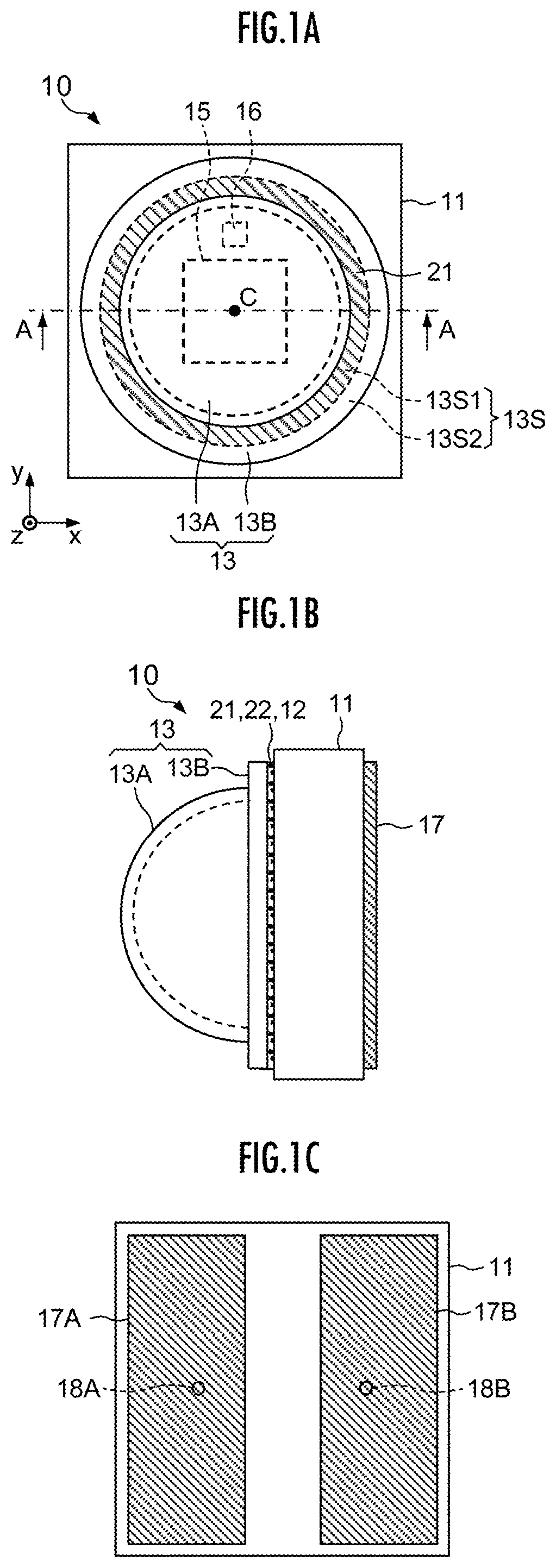
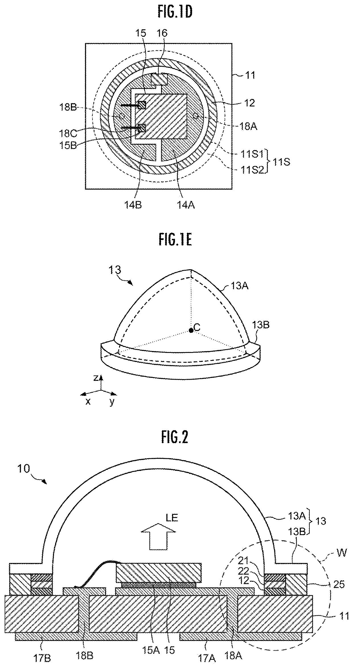
[0034]FIG. 1A is a plan view typically showing an upper surface of a semiconductor light emitting device 10 according to a first embodiment of the present invention. FIG. 1B is a view typically showing a side surface of the semiconductor light emitting device 10. FIG. 1C is a plan view typically showing a back surface of the semiconductor light emitting device 10. FIG. 1D is a view typically showing an internal structure of the semiconductor light emitting device 10. FIG. 2 is a cross-sectional view typically showing a cross-section of the semiconductor light emitting device 10 taken along line A-A of FIG. 1A.

[0035]As shown in FIGS. 1A and 1B, the semiconductor light emitting device 10 is comprised of a rectangular plate-shaped substrate 11 and a light transmitting cap 13 being a light transmissive window made of semispherical glass both being joined together. More specifically, an annular metal layer 12 (hereinafter also called a substrate metal layer 12) is formed on an upper surf...

second embodiment

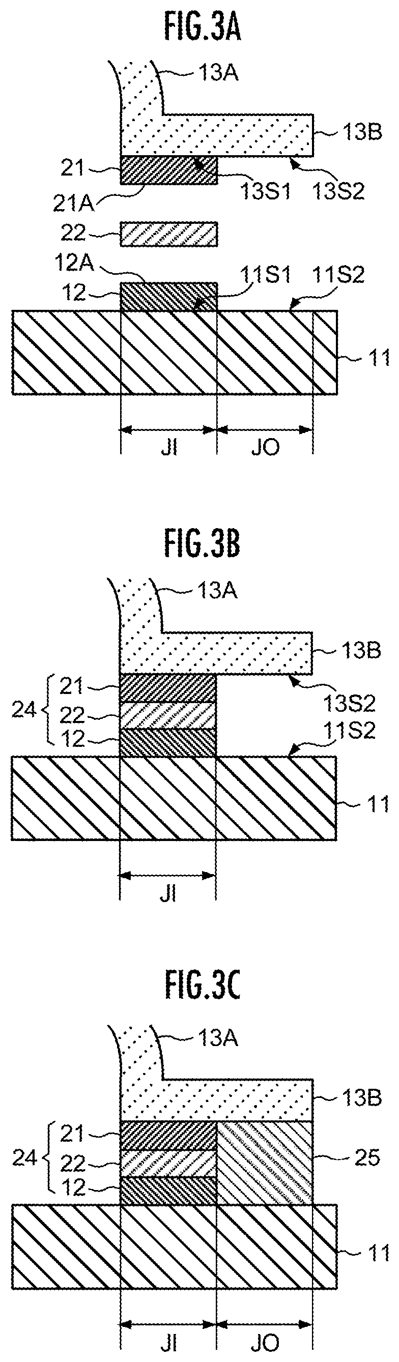
[0083]FIG. 4A is a view similar to FIG. 2 and is a cross-sectional view typically showing a cross-section of a semiconductor light emitting device 30 according to a second embodiment of the present invention. 4B is a partly enlarged cross-sectional view showing in an enlarge form, a joining part W between a substrate 11 and a light transmitting cap 13.

[0084]In the second embodiment, a flange part 13B of the light transmitting cap 13 has a flange protruding portion 13P which protrudes at an inner flange surface 13S1.

[0085]More specifically, the bottom surface (inner flange surface 13S1) of the flange protruding portion 13P has an annular shape, and a flange metal layer 21 is fixed to the inner flange surface 13S1.

[0086]Further, a substrate metal layer 12 is fixed to an inner annular-shaped region (an inner substrate joining surface) 11S1 of a substrate joining surface 11S. The substrate metal layer 12 and the flange metal layer 21 have shapes (annular shapes) and sizes corresponding ...

third embodiment

(Modified Examples of Third Embodiment)

[0099]FIGS. 6A and 6B are views similar to FIG. 5B and partly enlarged cross-sectional views showing in an enlarge form, a joining part W between a substrate 11 and a light transmitting cap 13 in each modified example of the third embodiment.

[0100]Referring to FIG. 6A, a groove GR is formed in an outer substrate joining surface 11S2. Also, referring to FIG. 6B, an inner groove GR1 and an outer groove GR2 (hereinafter collectively called a groove GR where there is no particular distinction) are formed in the outer substrate joining surface 11S2.

[0101]That is, at least one groove GR is formed in the outer substrate joining surface 11S2. The groove GR is formed as an annular groove (a groove of an outer ring) surrounding an inner joining part JI. Incidentally, the groove GR may be formed to be at least a part of the outer ring instead of a closed ring shape.

[0102]Then, an inorganic joining part 25 is formed so as to fill the at least one groove GR...


PUM

PropertyMeasurementUnit
wavelengthaaaaaaaaaa
light center wavelengthaaaaaaaaaa

Abstract

A semiconductor light emitting device includes a semiconductor light emitting element, a substrate mounted with the light emitting element and including a substrate joining surface having an inner substrate joining surface to which an annular-shaped substrate metal layer is fixed, and an outer substrate joining surface being an outer adjacent region of the inner substrate joining surface, and a light transmitting cap which has a window part transmitting light and a flange having a flange joining surface to which are annular-shaped flange metal layer is fixed, and which is sealed and joined to the substrate. A sealing joining section between the substrate and the cap has an inner joining part at which the substrate metal layer and the flange metal layer are joined by a metal joining material, and an outer joining part being an outer adjacent region of the inner joining part and being joined by an inorganic adhesive.

Description

BACKGROUND OF THE INVENTION1. Field of the Invention[0001]The present invention relates to a semiconductor light emitting device, and particularly to a semiconductor light emitting device having a semiconductor light emitting element enclosed thereinside which emits ultraviolet light.2. Description of the Related Art[0002]There has heretofore been known a semiconductor device having a semiconductor element enclosed inside a semiconductor package. In the case of a semiconductor light emitting module, a transparent window member such as glass which transmits light from a semiconductor light emitting element is joined to a support body mounted with the semiconductor light emitting element and airtightly sealed to each other.[0003]There has been disclosed in, for example, in Patent Literatures 1 (Japanese Patent Application Laid-Open No. 2015-18873) and 2 (Japanese Patent Application Laid-Open No. 2018-93137), a semiconductor light emitting module in which a substrate provided with a re...

Claims


Application Information

Patent Timeline
Patent Type & Authority Applications(United States)
IPC IPC(8): H01L33/38H01L33/32H01L33/20
CPCH01L33/382H01L33/20H01L33/32H01L33/58H01L33/56H01L33/54
Inventor IKEDA, KENJI
Owner STANLEY ELECTRIC CO LTD
Why Eureka
Try Eureka