Display panel and manufacturing method thereof

a technology of display panels and manufacturing methods, applied in the field of display panels, can solve problems such as damage to polyimide layers or other relevant layers, etc., and achieve the effects of preventing the movement of supporting structures, reducing the risk of alignment errors, and preventing abnormality of display panels

Inactive Publication Date: 2021-12-16
WUHAN CHINA STAR OPTOELECTRONICS TECH CO LTD
View PDF0 Cites 0 Cited by
  • Summary
  • Abstract
  • Description
  • Claims
  • Application Information

AI Technical Summary

Benefits of technology

[0005]The present disclosure provides a display panel and a manufacturing method thereof to solve a following problem: in conventional display panels, photo spacers are easy to be moved from a source / drain metal layer, contributing to abnormality of the display panels.
[0037]Embodiments of the present disclosure provide a display panel and a manufacturing method thereof. In the display panel, a first protrusion is formed on a side of an array substrate near a color filter substrate. As a result, when a supporting structure of a color filter substrate is aligned and attached to the array substrate, the first protrusion can be embedded into the supporting structure, thereby preventing the supporting structure from being moved. Therefore, risk of alignment error is reduced, and abnormality of the display panel is prevented.

Problems solved by technology

As a result, the photo spacers are easy to be moved from the source / drain metal layer, leading to a polyimide layer or other relevant layers being damaged, and contributing to abnormality of display panels.

Method used


Image

  • Display panel and manufacturing method thereof
  • Display panel and manufacturing method thereof
  • Display panel and manufacturing method thereof

Examples


Embodiment Construction

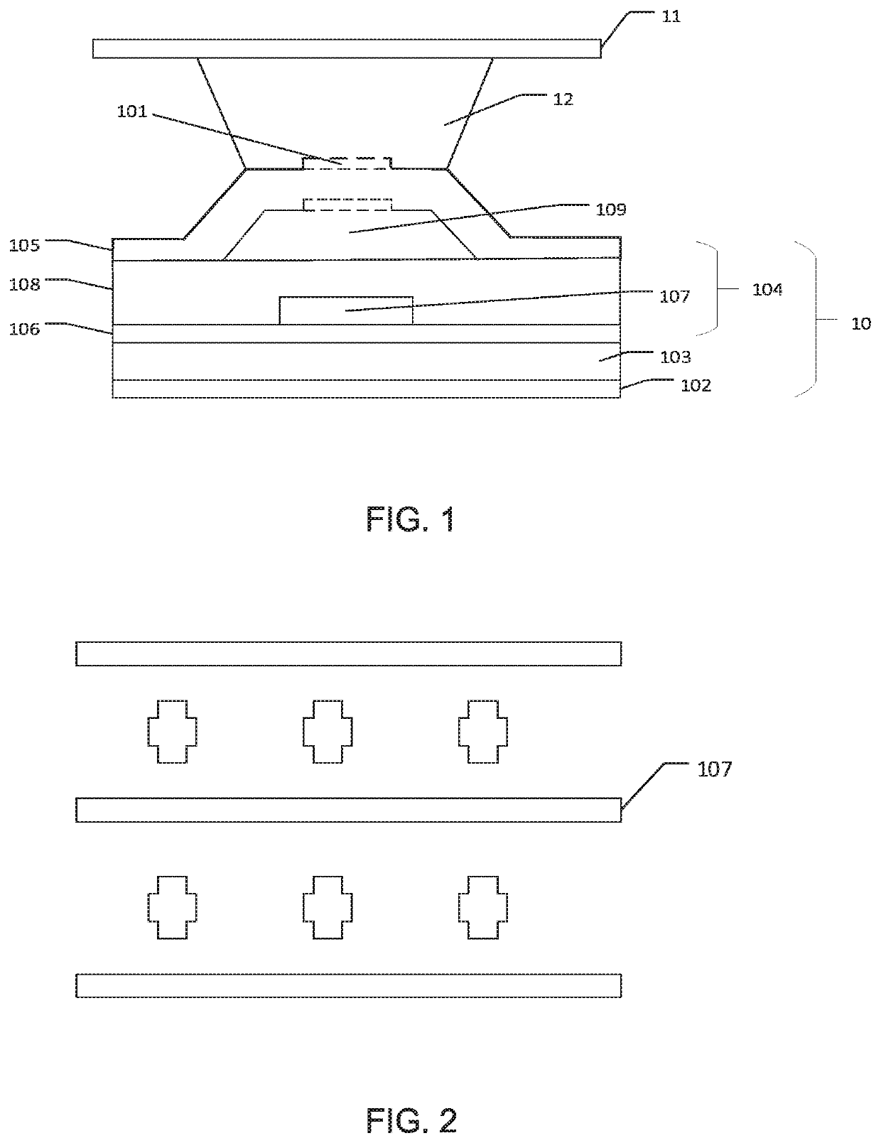
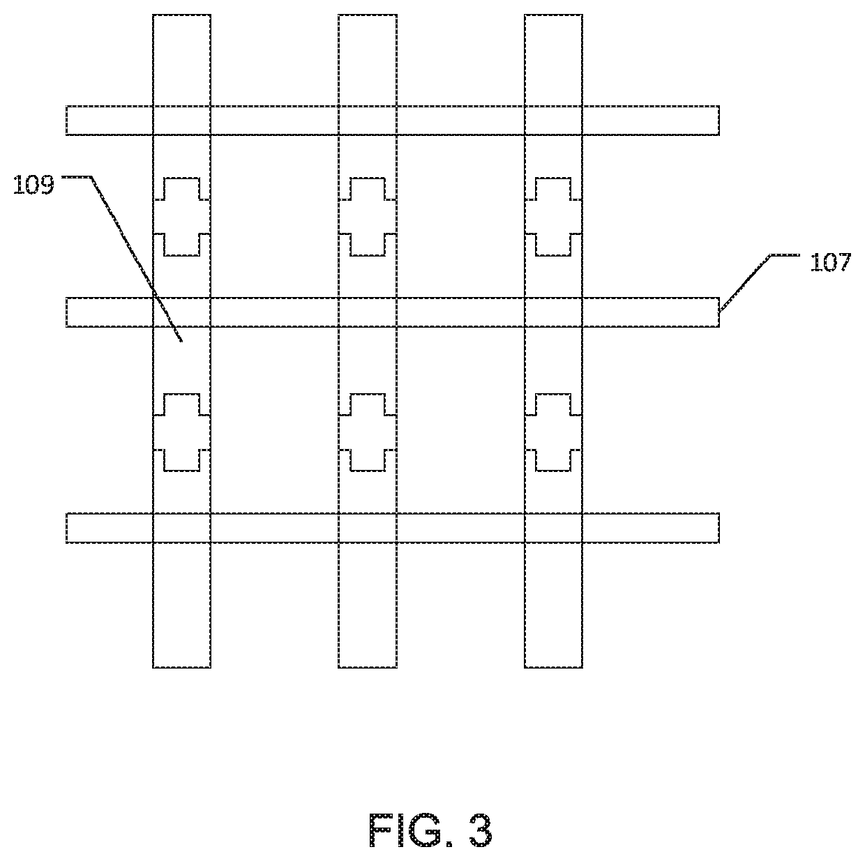
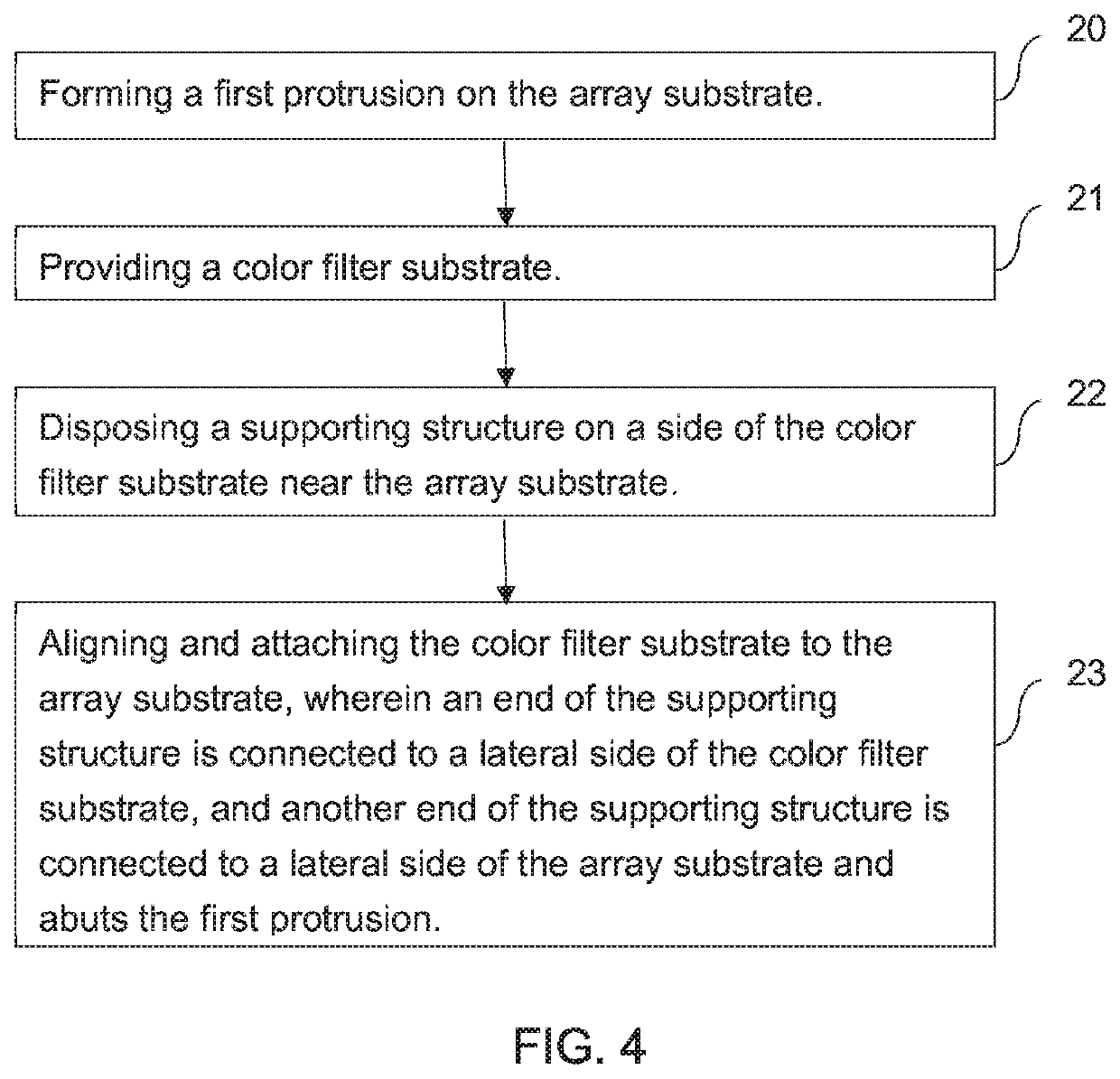
[0043]Hereinafter preferred embodiments of the present disclosure will be described with reference to the accompanying drawings to exemplify the embodiments of the present disclosure can be implemented, which can fully describe the technical contents of the present disclosure to make the technical content of the present disclosure clearer and easy to understand. However, the described embodiments are only some of the embodiments of the present disclosure, but not all of the embodiments. All other embodiments obtained by those skilled in the art based on the embodiments of the present disclosure without creative efforts are within the scope of the present disclosure.

[0044]In the description of the present disclosure, it should be understood that terms such as “center”, “longitudinal”, “lateral”, “length”, “width”, “thickness”, “upper”, “lower”, “front”, “rear”, “left”, “right”, “vertical”, “horizontal”, “top”, “bottom”, “inside”, “outside”, “clockwise”, “counter-clockwise”, as well a...


PUM

PropertyMeasurementUnit
sea level elevationaaaaaaaaaa
structuresaaaaaaaaaa
flexibleaaaaaaaaaa

Abstract

A display panel and a manufacturing method thereof are provided. The display panel includes: an array substrate with a first protrusion defined thereon; a color filter substrate disposed opposite to the array substrate; a supporting structure, wherein an end of the supporting structure is connected to a lateral side of the color filter substrate, another end of the supporting structure is connected to a lateral side of the array substrate, and the first protrusion is embedded into the supporting structure. The first protrusion is formed on a side of the array substrate near the color filter substrate. Therefore, when the supporting structure of the color filter substrate is aligned and attached to the array substrate, the first protrusion can be embedded into the supporting structure, thereby preventing the supporting structure from being moved. Thus, risk of alignment error is reduced, and abnormality of the display panel is prevented.

Description

RELATED APPLICATIONS[0001]This application claims the benefit of priority of Chinese Patent Application No. 202010524012.X filed on Jun. 10, 2020, the contents of which are incorporated herein by reference in their entirety.FIELDField and Background of the Invention[0002]The present disclosure relates to the field of display technologies, and more particularly, relates to a display panel and a manufacturing method thereof.[0003]Flat display devices, e.g., liquid crystal displays (LCDs), are widely used due to merits such as high resolution, low power consumption, thin and light body, and wide applications, and therefore have become mainstream display devices. Low temperature poly-silicon (LTPS) display technologies not only can prevent bright spots from appearing on panels, but also can increase resolution and reduce power consumption, which allows users to gain better visual experiences. To reduce manufacturing costs and production period of LTPS array substrates, an eight-mask pro...

Claims


Application Information

Patent Timeline
Patent Type & Authority Applications(United States)
IPC IPC(8): G02F1/1339H01L27/12H01L29/786H01L29/66G02F1/1368G02F1/1335
CPCG02F1/13394H01L27/1222H01L29/78618H01L29/78633H01L29/78678G02F2001/133302H01L27/1288H01L29/66765G02F1/1368G02F1/133514H01L27/1274G02F1/133345G02F1/1362G02F1/1333G02F1/133354G02F1/133302
Inventor AI, FEISONG, DEWEI
Owner WUHAN CHINA STAR OPTOELECTRONICS TECH CO LTD
Why Eureka
Try Eureka