Device for measuring overlay

a measurement device and overlay technology, applied in semiconductor/solid-state device testing/measurement, instruments, photomechanical equipment, etc., can solve the problems of overlay error between the two layers, failure to consider the difference in the magnification of the obtained waveform or image, and the performance and reliability of the manufactured circuit. to achieve the effect of accurately and quickly measuring an overlay error

Pending Publication Date: 2022-02-03
AUROS TECH
View PDF9 Cites 0 Cited by
  • Summary
  • Abstract
  • Description
  • Claims
  • Application Information

AI Technical Summary

Benefits of technology

[0015]According to the present invention, it is possible to provide an overlay measurement device capable of accurately and rapidly measuring an overlay error between layers having a large height difference and different optical properties.

Problems solved by technology

At this time, if the respective structures are not aligned within a tolerance range permitted in the manufacturing processes, interference may occur between the electrically activated patterns, and this phenomenon may cause problems in the performance and reliability of the manufactured circuit.
Thus, the overlay error between the two layers is measured.
However, this method has a problem in that the waveforms or images of the major scale 1 and the minor scale 2 are obtained through the use of the same beam without taking into account the fact that the major scale 1 and the minor scale 2 are formed of different materials in different layers and the major scale 1 is covered by the layer on which the minor scale 2 is formed.
In addition, there is a problem in that this method fails to consider the fact that the magnifications of the obtained waveforms or images are different because the heights of the major scale 1 and the minor scale 2 are different due to the height difference between the layer on which the major scale 1 is formed and the layer on which the minor scale 2 is formed.

Method used


Image

  • Device for measuring overlay
  • Device for measuring overlay
  • Device for measuring overlay

Examples


Embodiment Construction

[0027]Hereinafter, exemplary embodiments of the present invention will be described in detail with reference to the accompanying drawings. However, the embodiments of the present invention may be modified into various other forms, and the scope of the present invention should not be construed as being limited to the embodiments described below. Embodiments of the present invention are provided to more completely describe the present invention to those of ordinary skill in the art. Accordingly, the shapes of elements in the drawings are exaggerated in order to emphasize a more clear description. The elements indicated by the same reference numerals in the drawings mean the same elements.

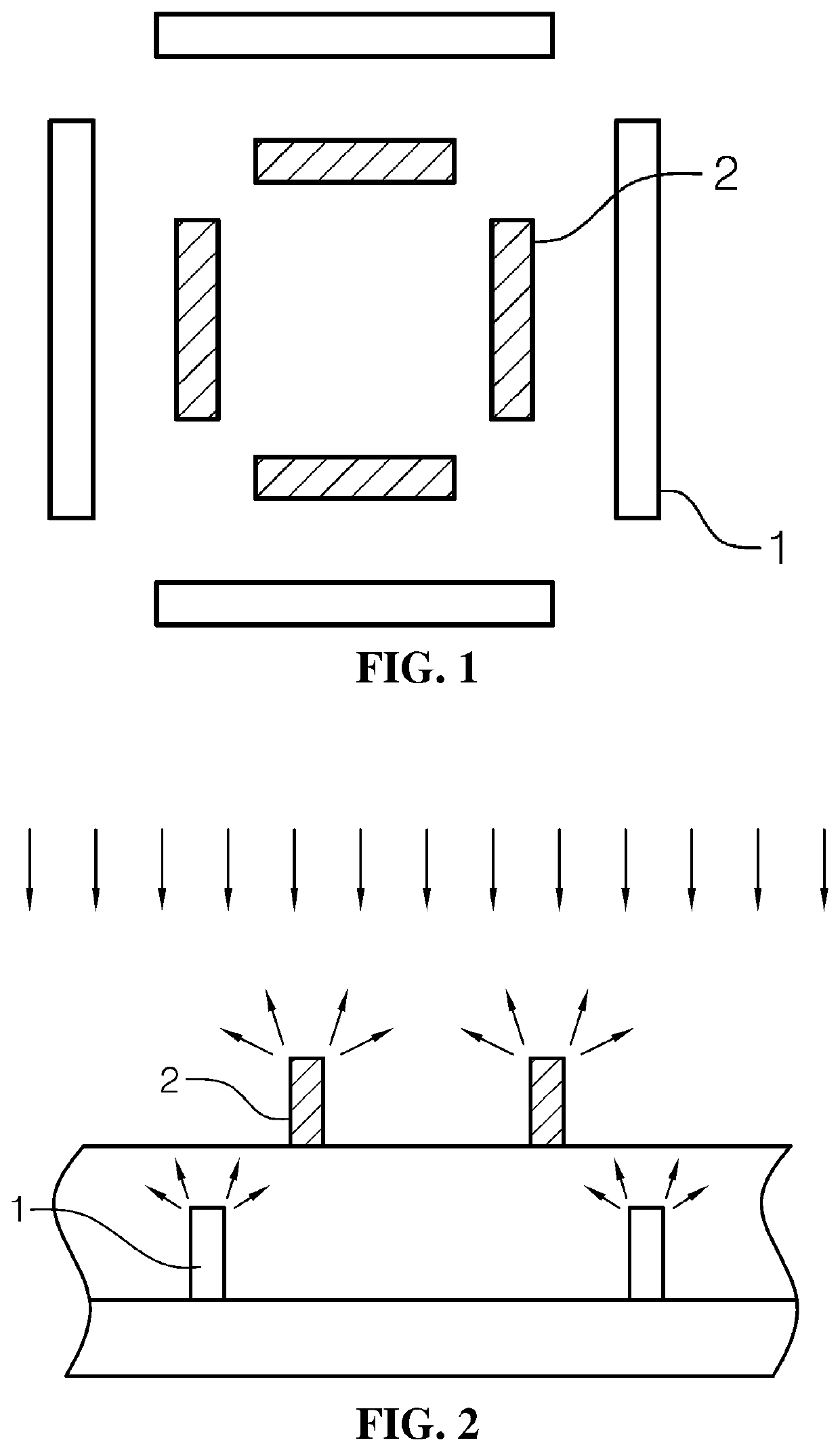
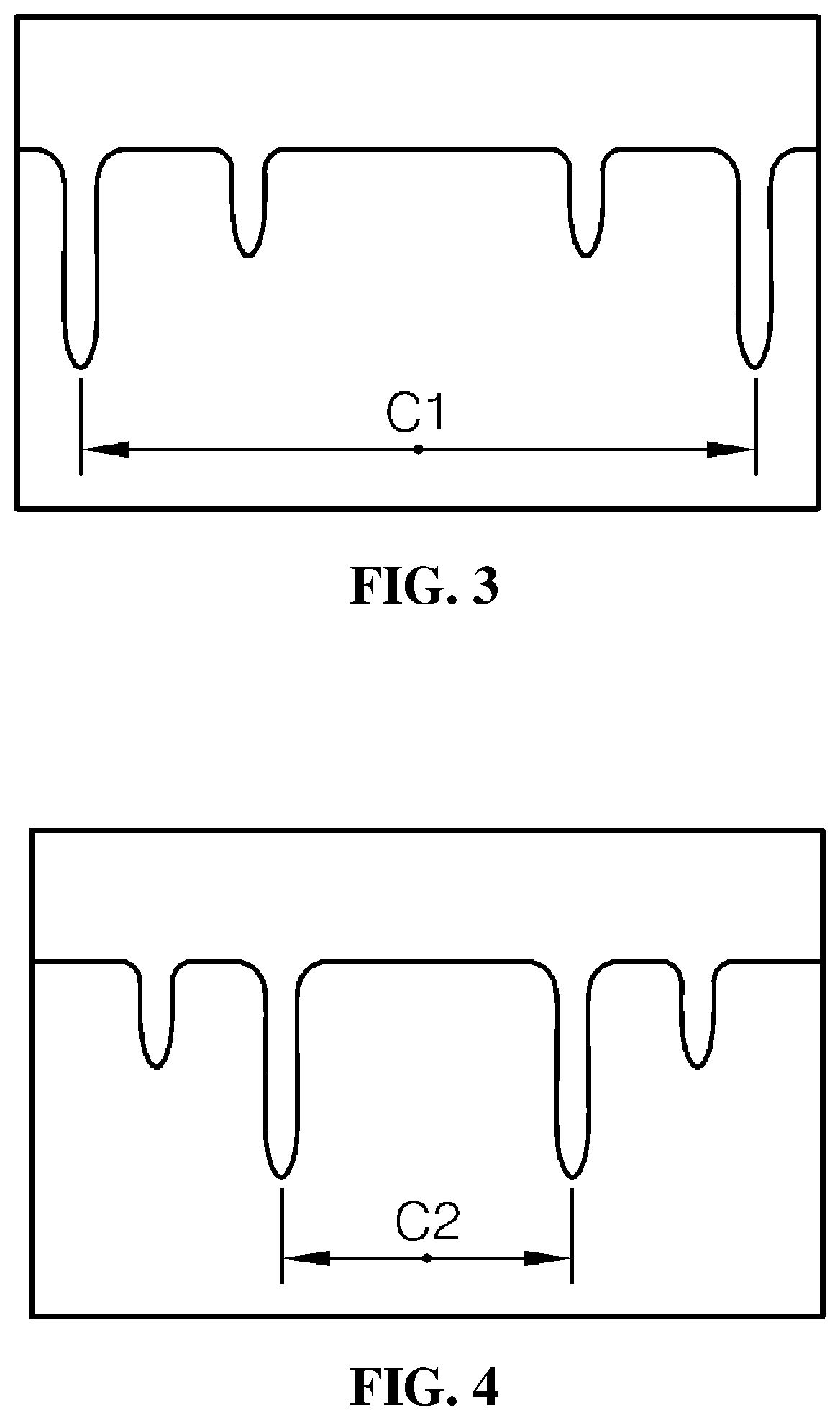
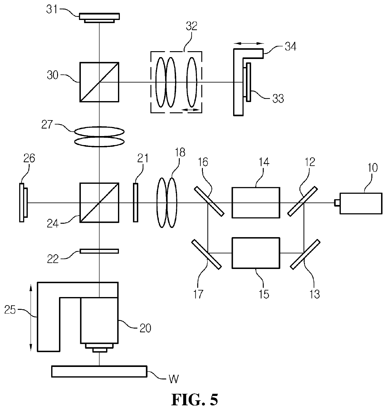
[0028]FIG. 5 is a conceptual diagram of an overlay measurement device according to an embodiment of the present invention. The overlay measurement device is a device that measures an error between a first overlay mark OM1 and a second overlay mark OM2 respectively formed on different layers formed on ...


PUM

PropertyMeasurementUnit
center wavelengthaaaaaaaaaa
band widthaaaaaaaaaa
distanceaaaaaaaaaa

Abstract

An overlay measurement device for measuring an error between a first overlay mark and a second overlay mark respectively formed on different layers formed on a wafer is proposed. The device includes a light source, a first beam splitter configured to split a beam emitted from the light source into two beams, a first color filter configured to adjust a center wavelength and a band width of one of the beams split by the first beam splitter so that the center wavelength and the band width of one of the beams become suitable for acquiring an image of the first overlay mark.

Description

TECHNICAL FIELD[0001]The present invention relates to an overlay measurement device.BACKGROUND ART[0002]As technology advances, the size of a semiconductor device is reduced, and an increase in the density of integrated circuits is required. In order to meet such a requirement, various conditions must be satisfied. Among these conditions, an overlay tolerance is one of the important indicators.[0003]Semiconductor devices are manufactured through numerous manufacturing processes. In order to form an integrated circuit on a wafer, it is necessary to go through a number of manufacturing processes so that desired circuit structures and elements are sequentially formed at specific locations. The manufacturing processes allow the sequential creation of patterned layers on the wafer. Electrically activated patterns are created in the integrated circuit through these repeated lamination processes. At this time, if the respective structures are not aligned within a tolerance range permitted ...

Claims


Application Information

Patent Timeline
Patent Type & Authority Applications(United States)
IPC IPC(8): G03F7/20G02B27/10G02B27/09
CPCG03F7/70633G02B27/0955G02B27/1006G03F7/70641G03F7/20G02B27/141G02B21/18G03F7/70775G03F7/70583H01L22/12
Inventor LEE, SUN HYOUNGLEE, KIL SOOLEE, SEUNG SOOPARK, GYU NAM
Owner AUROS TECH
Why Eureka
Try Eureka