Check patentability & draft patents in minutes with Patsnap Eureka AI!

Deep learning based defect detection

a deep learning and defect detection technology, applied in the field of methods and systems for detecting defects on specimens, can solve the problems of missing defects or false positives, requiring additional scanning time, and difficult defect detection

Active Publication Date: 2022-02-10
KLA TENCOR TECH CORP
View PDF2 Cites 3 Cited by
  • Summary
  • Abstract
  • Description
  • Claims
  • Application Information

AI Technical Summary

Benefits of technology

This patent describes a system and method for detecting defects on a specimen using a deep learning model. The system generates a gray scale simulated design data image from a high resolution image captured at the location on the specimen and detects the defects by subtracting the design data for that location from the simulated binary design data image. The technical effect of this patent is to provide a reliable and accurate tool for identifying defects on specimens, which can improve the efficiency and accuracy of manufacturing processes.

Problems solved by technology

However, as the dimensions of semiconductor devices decrease, inspection becomes even more important to the successful manufacture of acceptable semiconductor devices because smaller defects can cause the devices to fail.
Defect detection is often difficult due to factors such as image noise and subtleness of the defective pattern relative to the normal pattern.
One disadvantage of currently used methods, therefore, includes problems resulting from image noise and pattern noise that can result in missed defects or false positives.
SEM reference image subtraction can help but comes at a cost of additional scanning time.

Method used


Image

  • Deep learning based defect detection
  • Deep learning based defect detection
  • Deep learning based defect detection

Examples


Embodiment Construction

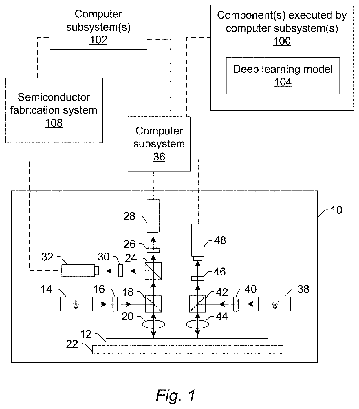
[0018]The terms “design,”“design data,” and “design information” as used interchangeably herein generally refer to the physical design (layout) of an IC or other semiconductor device and data derived from the physical design through complex simulation or simple geometric and Boolean operations. In addition, an image of a reticle acquired by a reticle inspection system and / or derivatives thereof can be used as a “proxy” or “proxies” for the design. Such a reticle image or a derivative thereof can serve as a substitute for the design layout in any embodiments described herein that use a design. The design may include any other design data or design data proxies described in commonly owned U.S. Pat. No. 7,570,796 issued on Aug. 4, 2009 to Zafar et al. and U.S. Pat. No. 7,676,077 issued on Mar. 9, 2010 to Kulkarni et al., both of which are incorporated by reference as if fully set forth herein. In addition, the design data can be standard cell library data, integrated layout data, desig...


PUM


Abstract

Methods and systems for detecting defects on a specimen are provided. One system includes one or more computer systems and one or more components executed by the one or more computer systems. The component(s) include a deep learning model configured for, for a location on a specimen, generating a gray scale simulated design data image from a high resolution image generated at the location by a high resolution imaging system. The computer system(s) are configured for generating a simulated binary design data image for the location from the gray scale simulated design data image. The computer system(s) are also configured for detecting defects at the location on the specimen by subtracting design data for the location from the simulated binary design data image.

Description

BACKGROUND OF THE INVENTION1. Field of the Invention[0001]The present invention generally relates to methods and systems for detecting defects on a specimen.2. Description of the Related Art[0002]The following description and examples are not admitted to be prior art by virtue of their inclusion in this section.[0003]Fabricating semiconductor devices such as logic and memory devices typically includes processing a substrate such as a semiconductor wafer using a large number of semiconductor fabrication processes to form various features and multiple levels of the semiconductor devices. For example, lithography is a semiconductor fabrication process that involves transferring a pattern from a reticle to a resist arranged on a semiconductor wafer. Additional examples of semiconductor fabrication processes include, but are not limited to, chemical-mechanical polishing (CMP), etch, deposition, and ion implantation. Multiple semiconductor devices may be fabricated in an arrangement on a ...

Claims


Application Information

Patent Timeline
Patent Type & Authority Applications(United States)
IPC IPC(8): G06T7/00G06K9/62G06T7/70G06T11/00G06N3/04G06N3/08
CPCG06T7/0006G06K9/6256G06T7/70G06T11/00G06T2207/10061G06N3/08G06T2207/30148G06T2207/20081G06N3/0454G06T7/001G06T2207/20084G06T2207/20224G06N3/088G06V2201/06G06V10/82G06N3/047G06N3/045G06F18/214G06T3/40G06N3/0475
Inventor WALLINGFORD, RICHARDCONG, GEPARK, SANGBONG
Owner KLA TENCOR TECH CORP
Features
  • R&D
  • Intellectual Property
  • Life Sciences
  • Materials
  • Tech Scout
  • Unparalleled Data Quality
  • Higher Quality Content
  • 60% Fewer Hallucinations
Learn More