Image sensor and image capturing apparatus
- Summary
- Abstract
- Description
- Claims
- Application Information
AI Technical Summary
Benefits of technology
Problems solved by technology
Method used
Image

Examples
first embodiment
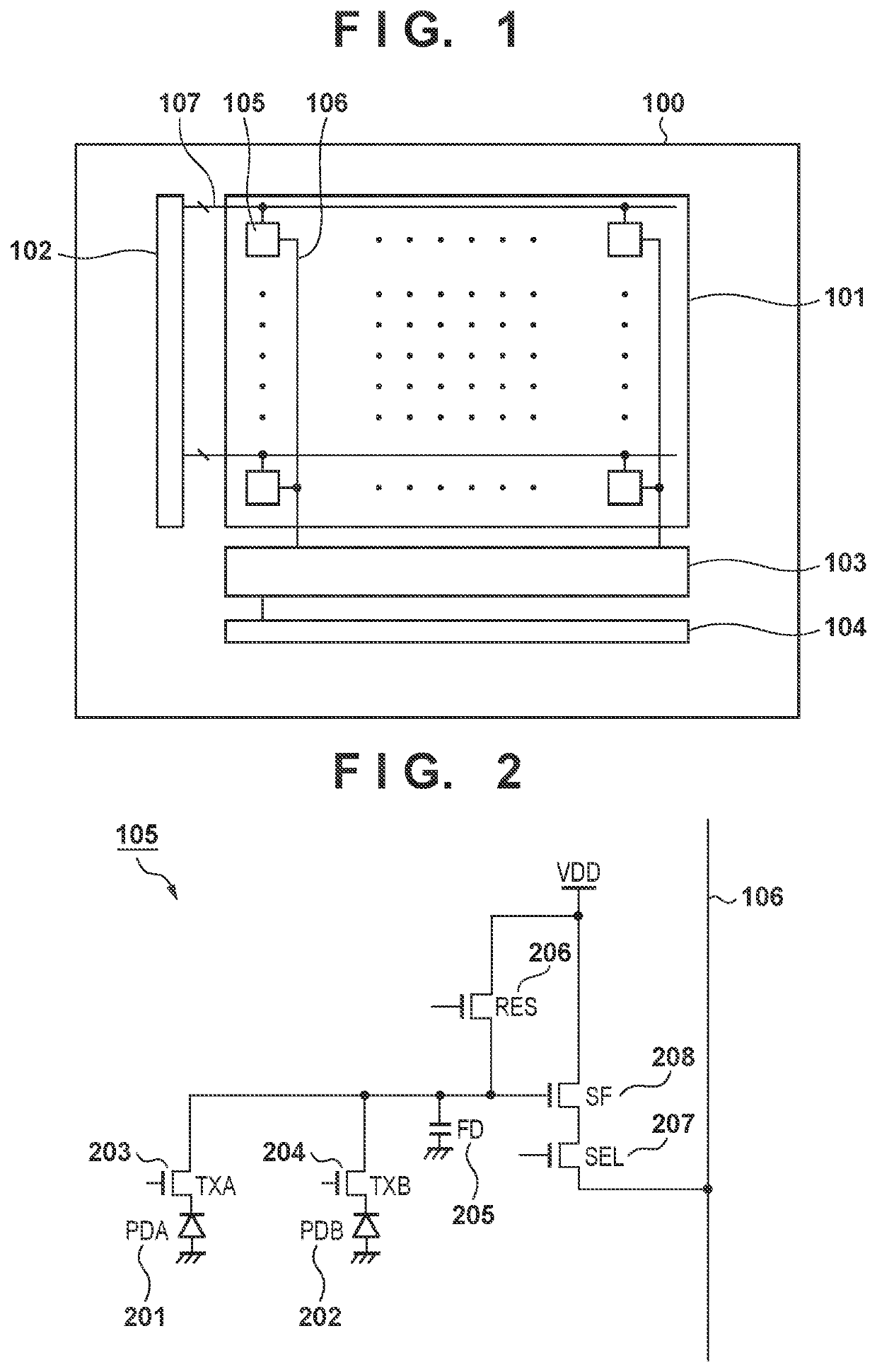
[0043]FIG. 1 is a diagram schematically showing the overall configuration of an image sensor 100 according to a first embodiment of the present invention. The image sensor 100 includes a pixel array 101 (pixel section), a vertical selection circuit 102, a column circuit 103, and a horizontal selection circuit 104.
[0044]A plurality of pixels 105 are arranged in a matrix in the pixel array 101. The outputs of the vertical selection circuit 102 are input to the pixels 105 via pixel drive wiring groups 107, and the pixel signals of the pixels 105 in a row selected by the vertical selection circuit 102 are read out to the column circuit 103 via output signal lines 106. One output signal line 106 may be provided for each pixel column or for a plurality of pixel columns, or a plurality of the output signal lines 106 may be provided for each pixel column. Signals read out in parallel through the plurality of output signal lines 106 are input to the column circuit 103, and the column circuit...
second embodiment
[0105]Next, a second embodiment of the present invention will be described.
[0106]In the second embodiment, a configuration in which a pixel signal reading circuit constituted with the FD 205 and its subsequent elements is shared by two pixels will be described. The constituents having the same functions as those in the first embodiment are designated by the same reference numerals, and detailed description thereof will be omitted or simplified.
[0107]FIG. 15 is an equivalent circuit diagram of two pixels in the second embodiment. In order to distinguish the photodiodes of the two pixels, the pixel on the upper side of the drawing is referred to as a pixel 105U and the two photodiodes of the pixel 105U are hereinafter referred to as PD1A 1501 and PD1B 1502. Further, the pixel on the lower side of the drawing is referred to as a pixel 105D and the two photodiodes of the pixel 105D are referred to as PD2A 1503 and PD2B 1504.
[0108]PD1A 1501 and PD1B 1502 share one microlens 301, and PD2A...
third embodiment
[0132]Next, a third embodiment of the present invention will be described.
[0133]FIG. 20 is a block diagram showing a schematic configuration of an image capturing apparatus according to the third embodiment of the present invention. The image capturing apparatus of the present embodiment includes an image sensor 100 having the configuration as described above, an overall control / arithmetic unit 2, an instruction unit 3, a timing generation unit 4, an imaging lens unit 5, a lens drive unit 6, a signal processing unit 7, a display unit 8 and a recording unit 9.
[0134]The imaging lens unit 5 forms an optical image of a subject on the image sensor 100. Although it is represented by one lens in the figure, the imaging lens unit 5 may include a plurality of lenses including a focus lens, a zoom lens, and a diaphragm, and may be detachable from the main body of the image capturing apparatus or may be integrally configured with the main body.
[0135]The image sensor 100 has the configuration a...
PUM
 Abstract
Description
Claims
Application Information
 - R&D Engineer
- R&D Manager
- IP Professional
- Industry Leading Data Capabilities
- Powerful AI technology
- Patent DNA Extraction
Browse by: Latest US Patents, China's latest patents, Technical Efficacy Thesaurus, Application Domain, Technology Topic.
© 2024 PatSnap. All rights reserved.Legal|Privacy policy|Modern Slavery Act Transparency Statement|Sitemap