Optical waveguide element and optical waveguide device

a technology of optical waveguide and element, applied in the direction of optics, printed circuit details, instruments, etc., can solve the problems of reducing manufacturing yield and new problems, and achieve the effects of preventing substrate cracking, reducing manufacturing yield, and preventing connection failur

Pending Publication Date: 2022-02-24
SUMITOMO OSAKA CEMENT CO LTD
View PDF0 Cites 0 Cited by
  • Summary
  • Abstract
  • Description
  • Claims
  • Application Information

AI Technical Summary

Benefits of technology

[0023]According to the present invention, in an optical waveguide element using a thinly processed substrate such as a rib-type optical modulation element, it is possible to prevent substrate cracking at the time of electrical connection such as wire bonding in which a pressure is applied to the substrate and thus to prevent a connection failure and a reduction in manufacturing yield.

Problems solved by technology

However, as a result of the substrate being thinnly processed to a thickness of about several tens of microns, a new problem may occur.
That is, an optical modulation element of the related art using a thin substrate such as a rib-type optical modulation element may cause a problem such as a decrease in manufacturing yield due to poor connection with an electric component or the like.

Method used


Image

  • Optical waveguide element and optical waveguide device
  • Optical waveguide element and optical waveguide device
  • Optical waveguide element and optical waveguide device

Examples


Embodiment Construction

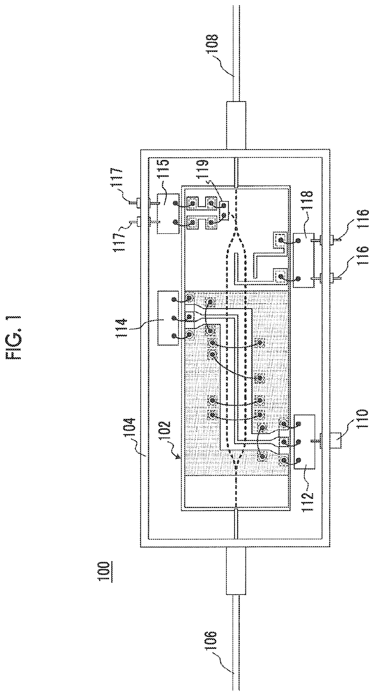
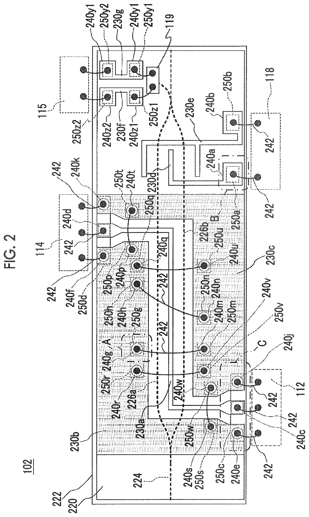
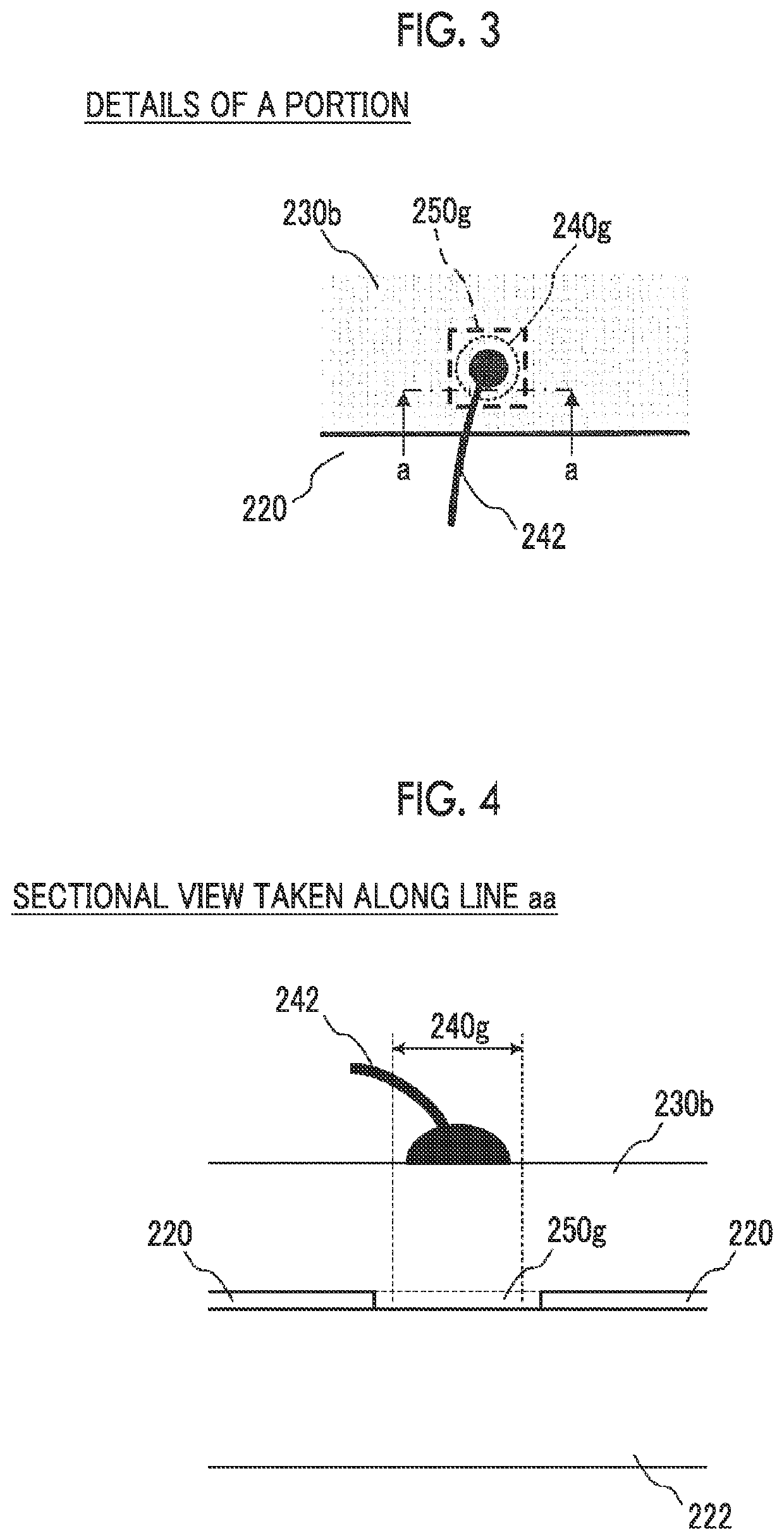
[0041]Hereinafter, embodiments of the present invention will be described with reference to the drawings. An optical waveguide element according to the embodiments described below is an optical modulation element configured by using an LN substrate, but the optical waveguide element according to the present invention is not limited to this. The present invention can be similarly applied to an optical waveguide element having an electrode using a substrate having an electro-optic effect, a thermo-optic effect, and an acoustic-optic effect in addition to the LN substrate, and an optical waveguide element having a function other than optical modulation.

[0042]FIG. 1 is a diagram illustrating a configuration of an optical waveguide element and an optical waveguide device according to an embodiment of the present invention. In the present embodiment, the optical waveguide element is an optical modulation element 102 that performs optical modulation by using a Mach-Zehnder optical waveguid...


PUM

PropertyMeasurementUnit
diameteraaaaaaaaaa
thicknessaaaaaaaaaa
sizeaaaaaaaaaa

Abstract

In an optical modulation element using a thinly processed substrate, cracking of the substrate during electrical connection is prevented, and poor connection or a reduction in manufacturing yield is prevented. An optical waveguide element includes an optical substrate on which an optical waveguide and a conductor pattern are formed, and a support substrate that supports the optical substrate, in which the conductor pattern includes at least one electrical connection area defined as a range in which electrical connection is performed, the optical substrate has a substrate removal portion in which a material of the optical substrate has been removed to penetrate through the optical substrate at a portion corresponding to the electrical connection area, and at least a part of the electrical connection area is formed on the support substrate via the substrate removal portion.

Description

TECHNICAL FIELD[0001]The present invention relates to an optical waveguide element and an optical waveguide device.BACKGROUND ART[0002]In high-speed / large-capacity optical fiber communication systems, optical transmission apparatuses incorporating a waveguide type optical modulator are often used. Above all, an optical modulation element using LiNbO3 (hereinafter, also referred to as LN) having an electro-optic effect for a substrate has less light loss and can realize a wide-band optical modulation characteristic compared with a modulation element using a semiconductor-based material such as indium phosphide (InP), silicon (Si), or gallium arsenide (GaAs), and is thus widely used in high-speed / large-capacity optical fiber communication systems.[0003]On the other hand, in a modulation method in an optical fiber communication system, multi-level modulation such as quadrature phase shift keying (QPSK) or dual polarization-quadrature phase shift keying (DP-QPSK) or transmission formats...

Claims


Application Information

Patent Timeline
Patent Type & Authority Applications(United States)
IPC IPC(8): G02F1/035
CPCG02F1/0356G02F1/035H05K1/02
Inventor MOTOYA, MASAYUKIMIYAZAKI, NORIKAZU
Owner SUMITOMO OSAKA CEMENT CO LTD
Why Eureka
Try Eureka