
Electrophoretic display device and manufacturing method thereof

a display device and display technology, applied in the field of display devices and manufacturing methods thereof, can solve the problems of increasing manufacturing costs, not allowing the display to perform a partial update, and not being suitable for manufacturers capable of only one photomask manufacturing process

Pending Publication Date: 2022-02-24
E INK HLDG INC
View PDF1 Cites 0 Cited by
  • Summary
  • Abstract
  • Description
  • Claims
  • Application Information

AI Technical Summary

Benefits of technology

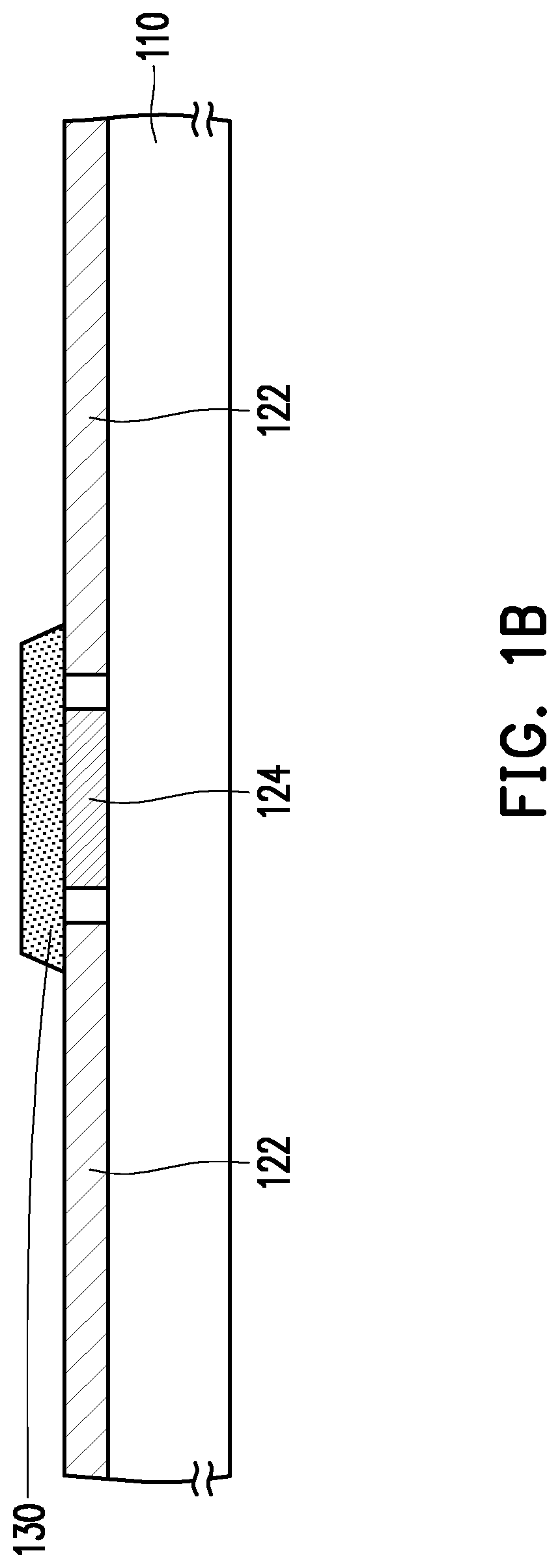
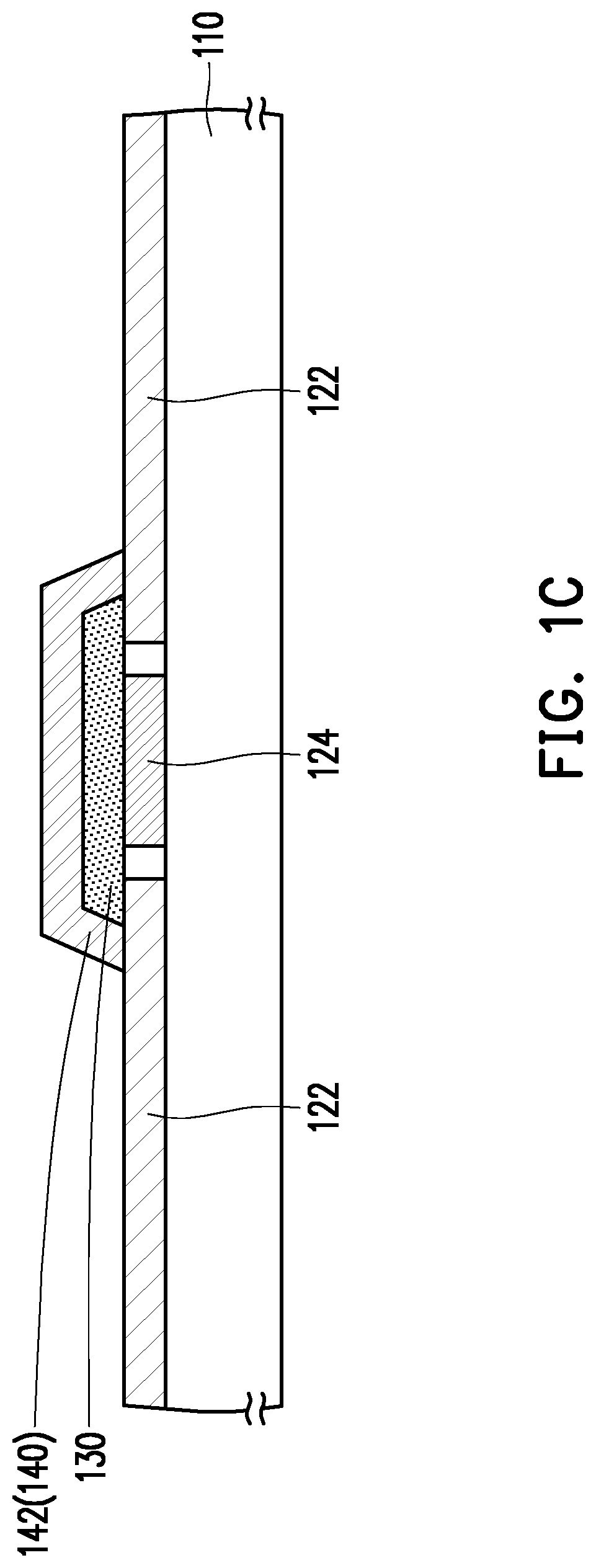
The disclosure provides an electrophoretic display device that prevents the occurrence of signal line traces without increasing the number of photomasks and having a lower manufacturing process cost. The method involves forming insulating patterns using screen printing and then conductive patterns that cover the insulating patterns and bridge to the adjacent background patterns. This results in a second conductive layer with the same potential as the background patterns, shielding the electric field generated by the signal lines and preventing the generation of signal line traces. Overall, the method reduces the number of masks and lowers the manufacturing process cost.

Problems solved by technology

The above-mentioned solution may make a product price competitive, but it does not allow the display to perform a partial update.
However, the above-mentioned solution requires additional driver chips for driving, such as a plastic package or a chip on film (COF), therefore increasing the manufacturing cost.
However, in addition to the three photomask manufacturing processes being time-consuming and costly, it is not suitable for manufacturers capable of only one photomask manufacturing process.

Method used


Image

  • Electrophoretic display device and manufacturing method thereof
  • Electrophoretic display device and manufacturing method thereof
  • Electrophoretic display device and manufacturing method thereof

Examples


Embodiment Construction

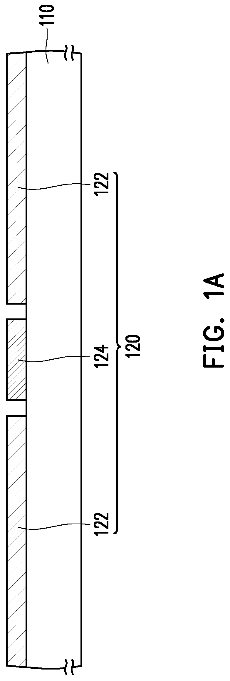
[0021]FIGS. 1A to 1D are cross-sectional schematic views of a manufacturing method of an electrophoretic display device according to an embodiment of the disclosure. FIGS. 2A to 2C are top schematic views of FIGS. 1A to 1C, respectively. It should be noted that FIGS. 1A to 1C are cross-sectional schematic views taken along line I-I in FIGS. 2A to 2C, respectively.

[0022]First of all, with reference to FIGS. 1A and 2A concurrently, in a manufacturing method of the electrophoretic display device of the embodiment, a first conductive layer 120 is formed on a substrate 110. The method of forming the first conductive layer 120 includes performing a process of photoresist coating, exposure, development, and etching. That is, the first conductive layer 120 is formed by photolithography. Furthermore, the first conductive layer 120 of the embodiment includes multiple background patterns 122 and multiple signal lines 124. Each of the signal lines 124 is located between two adjacent background ...


PUM

PropertyMeasurementUnit
conductiveaaaaaaaaaa
colorsaaaaaaaaaa
durabilityaaaaaaaaaa

Abstract

An electrophoretic display device, including a substrate, a first conductive layer, multiple insulating patterns, a second conductive layer, an adhesive layer, and an electrophoretic display film, is provided. The first conductive layer is disposed on the substrate, and includes multiple background patterns and multiple signal lines. Each of the signal lines is located between two adjacent background patterns. Each of the insulating patterns covers each of the signal lines and bridges to the two adjacent background patterns. The second conductive layer includes multiple conductive patterns. Each of the conductive patterns covers the each of the insulating patterns and bridges to the two adjacent background patterns. The adhesive layer is disposed on and in direct contact with the background pattern and the second conductive layer. The electrophoretic display film is disposed above the adhesive layer.

Description

CROSS-REFERENCE TO RELATED APPLICATION[0001]This application claims the priority benefit of Taiwan application serial no. 109128358, filed on Aug. 20, 2020. The entirety of the above-mentioned patent application is hereby incorporated by reference herein and made a part of this specification.BACKGROUNDTechnical Field[0002]This disclosure relates to a display device and a manufacturing method thereof, and in particular to an electrophoretic display device and a manufacturing method thereof.Description of Related Art[0003]In general, a segmented electronic paper display has characteristics such as ultra-low power consumption, thinness, and durability. The segmented electronic paper display can display content clearly in direct sunlight, and the screen can still be displayed even when it is not connected to a power source. In a currently available segmented electrophoretic display, trace line marks in a background region, that is, traces of data lines, are reduced by controlling the wa...

Claims


Application Information

Patent Timeline
Patent Type & Authority Applications(United States)
IPC IPC(8): G02F1/16756G02F1/167G02F1/16755G02F1/1676G02F1/1679
CPCG02F1/16756G02F1/167G02F1/1679G02F1/1676G02F1/16755G02F1/1685
Inventor CHENG, HSIAO-LUNGTIEN, PEI-LINLO, I-SHINHUNG, CHI-MAO
Owner E INK HLDG INC
Learn More