Display apparatus
a display apparatus and display technology, applied in the field of spliced display apparatuses, can solve the problems of solving the foregoing problem and reducing the difficulty of repairing the display apparatus, and achieve the effect of favorable display quality and production yield
- Summary
- Abstract
- Description
- Claims
- Application Information
AI Technical Summary
Benefits of technology
Problems solved by technology
Method used
Image
Examples
first embodiment
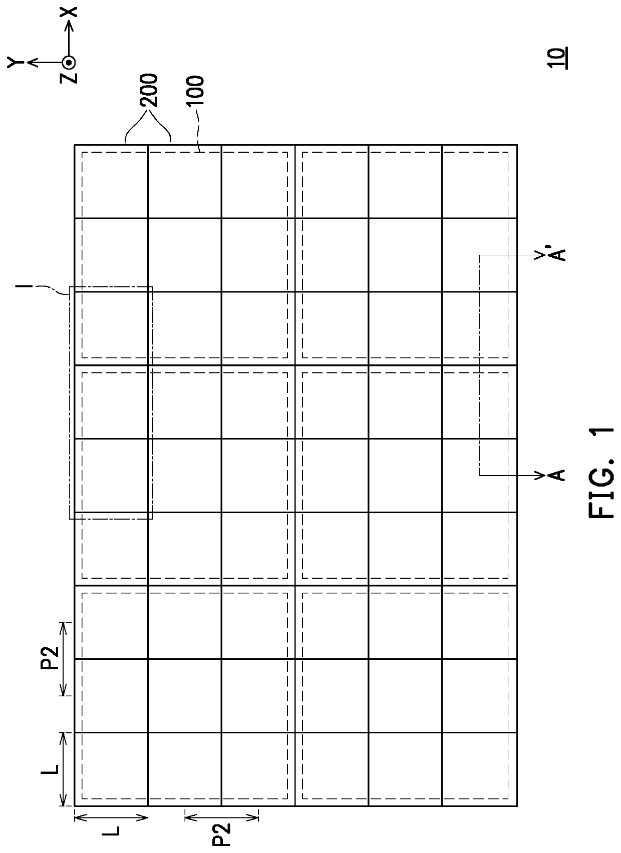
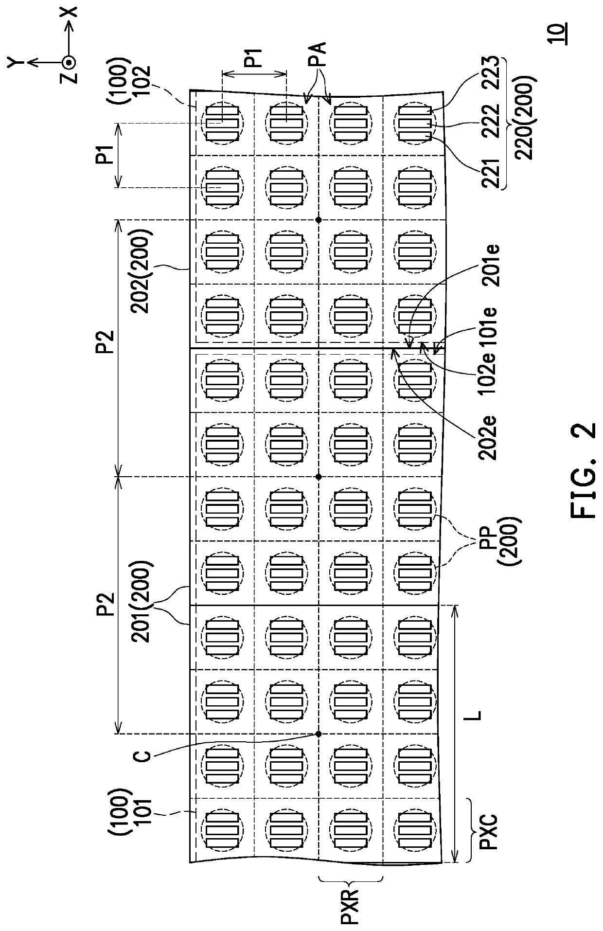
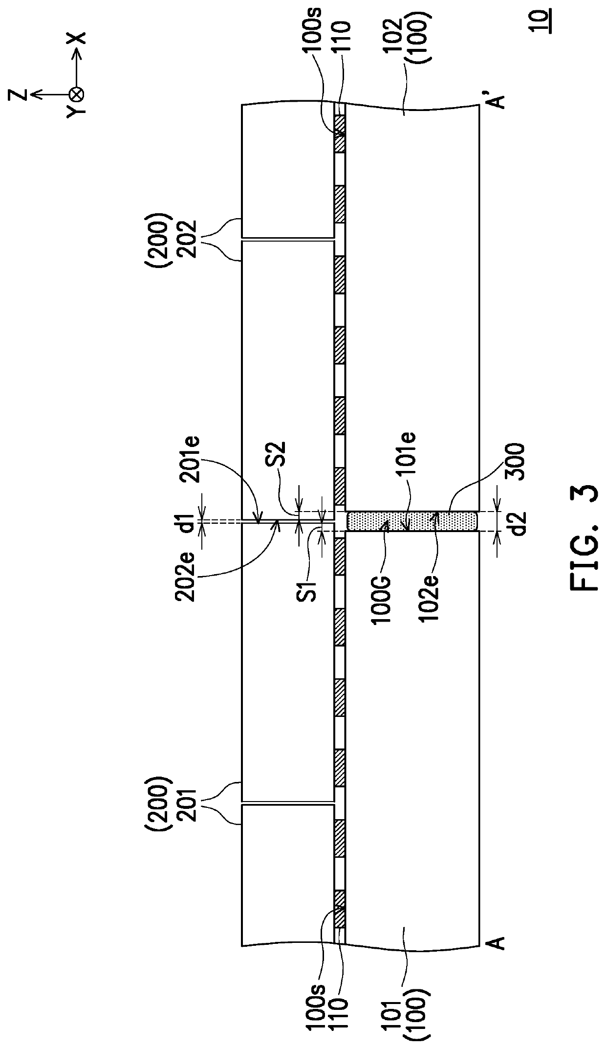
[0034]FIG. 1 is a front schematic view of a display apparatus according to the disclosure. FIG. 2 is an enlarged schematic view of a local region of the display apparatus of FIG. 1. FIG. 2 corresponds to a region I of FIG. 1. FIG. 3 is a cross-sectional schematic view of the display apparatus of FIG. 1. FIG. 3 corresponds to a cross-sectional line A-A′ of FIG. 1. FIG. 4 is a cross-sectional schematic view of light emitting display units of FIG. 1. FIG. 5 is a front schematic view of a display apparatus according to another embodiment of the disclosure. For clarity and description, only a light emitting device 220 and a pad structure PP of FIG. 4 are illustrated in a light emitting display unit 200 of FIG. 2, and illustration of detailed members of the light emitting display unit 200 of FIG. 4 is omitted in FIG. 3.
[0035]With reference to FIG. 1 to FIG. 4, a display apparatus 10 includes a plurality of circuit boards 100 and a plurality of light emitting display units 200. These light...
second embodiment
[0059]FIG. 6 is a cross-sectional schematic view of a display apparatus according to the disclosure. With reference to FIG. 6, a difference between a display apparatus 10B of this embodiment and the display apparatus 10 of FIG. 3 is that: light emitting display units 200′ of the display apparatus 10B are required to be processed through a cutting process before being transposed to the circuit boards 100. That is, in this embodiment, a clearly visible gap G is provided between any adjacent two of the light emitting display units 200′ located on the same circuit board 100. This gap G may act as a buffering space of the light emitting display units 200′ for volume expansion caused by heating during a transposition and bonding process, and a transfer yield of the light emitting display units 200′ may thus be increased. Note that a spacing S3 of the gap G between any adjacent two light emitting display units 201′ (or light emitting display units 202′) in an arrangement direction (e.g., d...
third embodiment
[0062]FIG. 7 is a front schematic view of a display apparatus according to the disclosure. FIG. 8 is an enlarged schematic view of a local region of the display apparatus of FIG. 7. FIG. 8 corresponds to a region II of FIG. 7. FIG. 9 is a cross-sectional schematic view of the display apparatus of FIG. 7. FIG. 9 corresponds to a cross-sectional line B-B′ of FIG. 7.
[0063]With reference to FIG. 7 to FIG. 9, a difference between a display apparatus 20 of this embodiment and the display apparatus 10 of FIG. 1 is that: the display apparatus 20 provides a different structure and a different shape. To be specific, in the visual direction (e.g., direction Z), an outer contour of the display apparatus 20 is non-rectangular, and the non-rectangular contour is formed by splicing of two circuit boards of different sizes. In this embodiment, the display apparatus 20 includes a plurality of circuit boards 100A and a plurality of circuit boards 100B, and sizes of the circuit boards 100A are greater...
PUM
| Property | Measurement | Unit |
|---|---|---|
| thickness | aaaaa | aaaaa |
| length | aaaaa | aaaaa |
| distance d1 | aaaaa | aaaaa |
Abstract
Description
Claims
Application Information
 - R&D
- Intellectual Property
- Life Sciences
- Materials
- Tech Scout
- Unparalleled Data Quality
- Higher Quality Content
- 60% Fewer Hallucinations
Browse by: Latest US Patents, China's latest patents, Technical Efficacy Thesaurus, Application Domain, Technology Topic, Popular Technical Reports.
© 2025 PatSnap. All rights reserved.Legal|Privacy policy|Modern Slavery Act Transparency Statement|Sitemap|About US| Contact US: help@patsnap.com


