Wafer processing method

a processing method and wafer technology, applied in the direction of semiconductor devices, electrical equipment, semiconductor/solid-state device testing/measurement, etc., can solve the problems of reducing the quality of the device chip due to the residue of the adhesive, and causing the bump to be damaged

Pending Publication Date: 2022-03-03
DISCO CORP
View PDF9 Cites 0 Cited by
  • Summary
  • Abstract
  • Description
  • Claims
  • Application Information

AI Technical Summary

Benefits of technology

[0011]In the wafer processing method according to one mode of the present invention, it is determined whether or not a residue of the protective member is present, after the protective member is peeled off from the wafer. As a result, it becomes possibl

Problems solved by technology

For example, when a portion of the adhesive is left in the state of being deposited on the bump of the device, defective connection of the bump may be generated when the device chip obtained by the division of the wafer is mounted to a mounting substrate.
Therefore, a lowering in the quality of

Method used


Image

  • Wafer processing method
  • Wafer processing method
  • Wafer processing method

Examples


Embodiment Construction

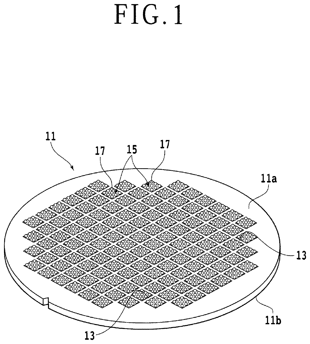
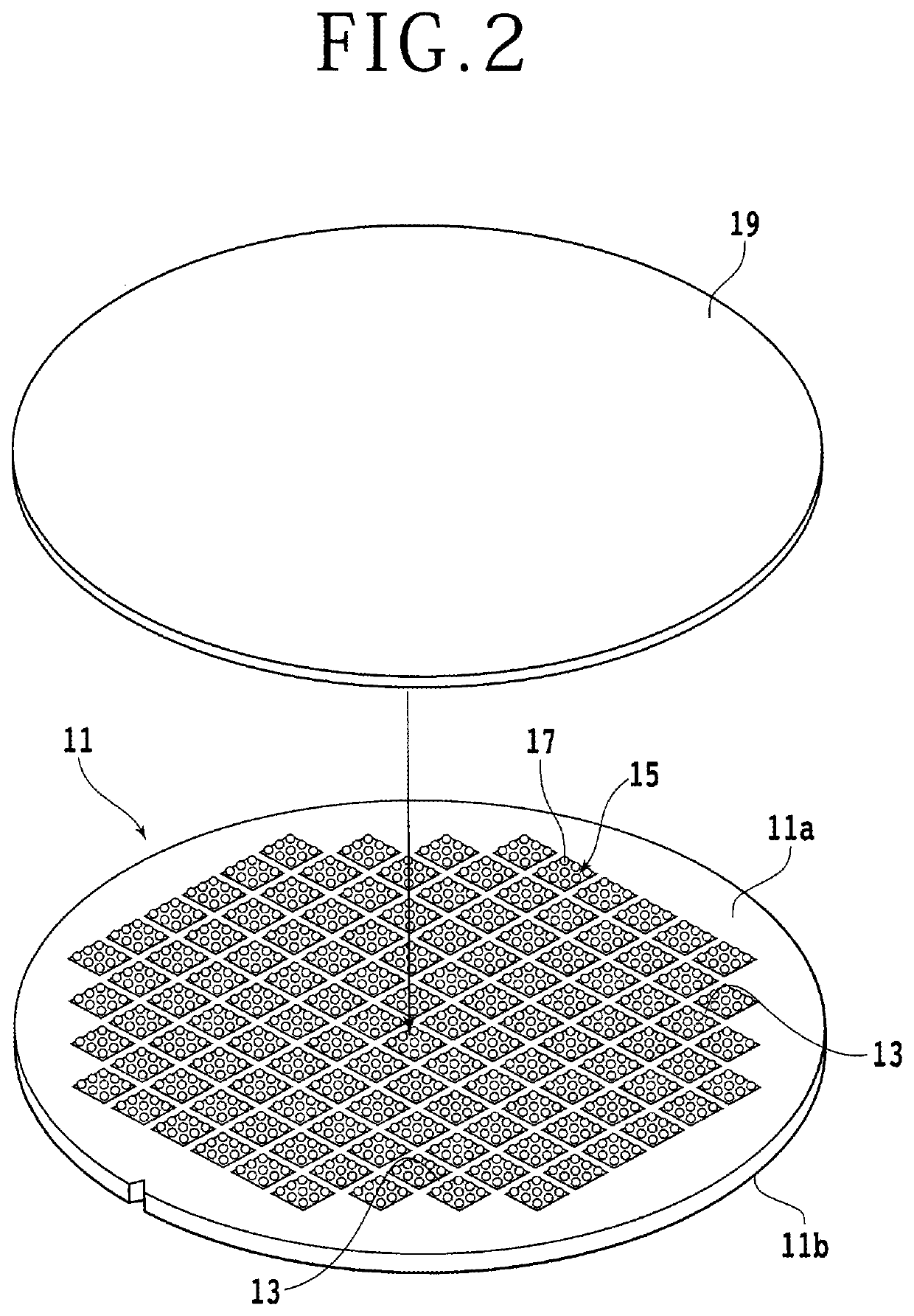
[0025]An embodiment according to one mode of the present invention will be described below referring to the attached drawings. First, a configuration example of a wafer processed by a wafer processing method according to the present invention will be described. FIG. 1 is a perspective view depicting a wafer 11.

[0026]The wafer 11 is, for example, a disk-shaped substrate including a semiconductor such as silicon, and has a front surface (first surface) 11a and a back surface (second surface) 11b which are substantially parallel to each other. The wafer 11 is partitioned into a plurality of rectangular regions by a plurality of streets 13 arranged in a grid pattern such as to intersect each other. On the front surface 11a side of the plurality of regions partitioned by the streets 13, devices 15 such as an integrated circuit (IC), large scale integration (LSI), a light emitting diode (LED), and micro electro mechanical systems (MEMS) are formed. Note that a material, a shape, a structu...


PUM


Abstract

A wafer processing method for processing a back surface side of a wafer having ruggedness on a front surface side includes a protective member disposing step of putting a protective member in close contact with the front surface side of the wafer along the ruggedness and covering the front surface side of the wafer with the protective member, a processing step of holding the protective member side of the wafer by a chuck table and processing the back surface side of the wafer, a protective member peeling step of peeling off the protective member from the front surface side of the wafer, and a residue determination step of determining whether or not a residue of the protective member is present on the front surface side of the wafer and recording a determination result on the wafer basis.

Description

BACKGROUND OF THE INVENTIONField of the Invention[0001]The present invention relates to a wafer processing method for covering a wafer with a protective member and processing the wafer.Description of the Related Art[0002]In a manufacturing process of device chips, a wafer formed with devices in a plurality of regions partitioned by a plurality of streets arranged in a grid pattern is used. The wafer is divided along the streets, whereby a plurality of device chips including the devices respectively are obtained. The device chips are assembled into various electronic apparatuses such as mobile phones and personal computers.[0003]For the cutting of the wafer, for example, a cutting apparatus is used. The cutting apparatus includes a holding table that holds a workpiece, and a cutting unit to which an annular cutting blade for cutting the workpiece is mounted. The wafer is held by the holding table and the cutting blade is rotated and is made to cut into the wafer, whereby the wafer is...

Claims


Application Information

Patent Timeline
IPC IPC(8): H01L21/683H01L21/78H01L21/67
CPCH01L21/6836H01L21/67132H01L21/78H01L22/12H01L21/02076H01L2221/68327H01L2221/6834H01L2221/68386H01L21/304H01L21/67288H01L2221/68381
Inventor SAKAILAN, HEIDI
Owner DISCO CORP
Why Eureka
Try Eureka