

Method for transferring a surface layer to cavities
- Summary
- Abstract
- Description
- Claims
- Application Information
AI Technical Summary
Benefits of technology
Problems solved by technology
Method used
Image

Examples
example of an embodiment
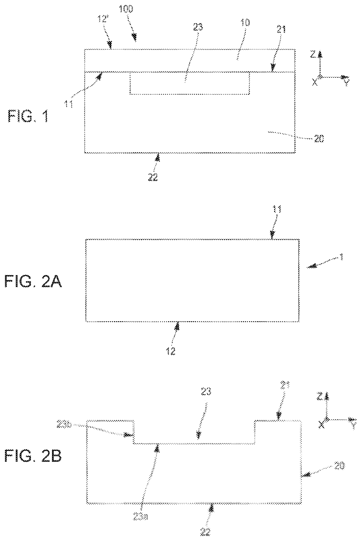
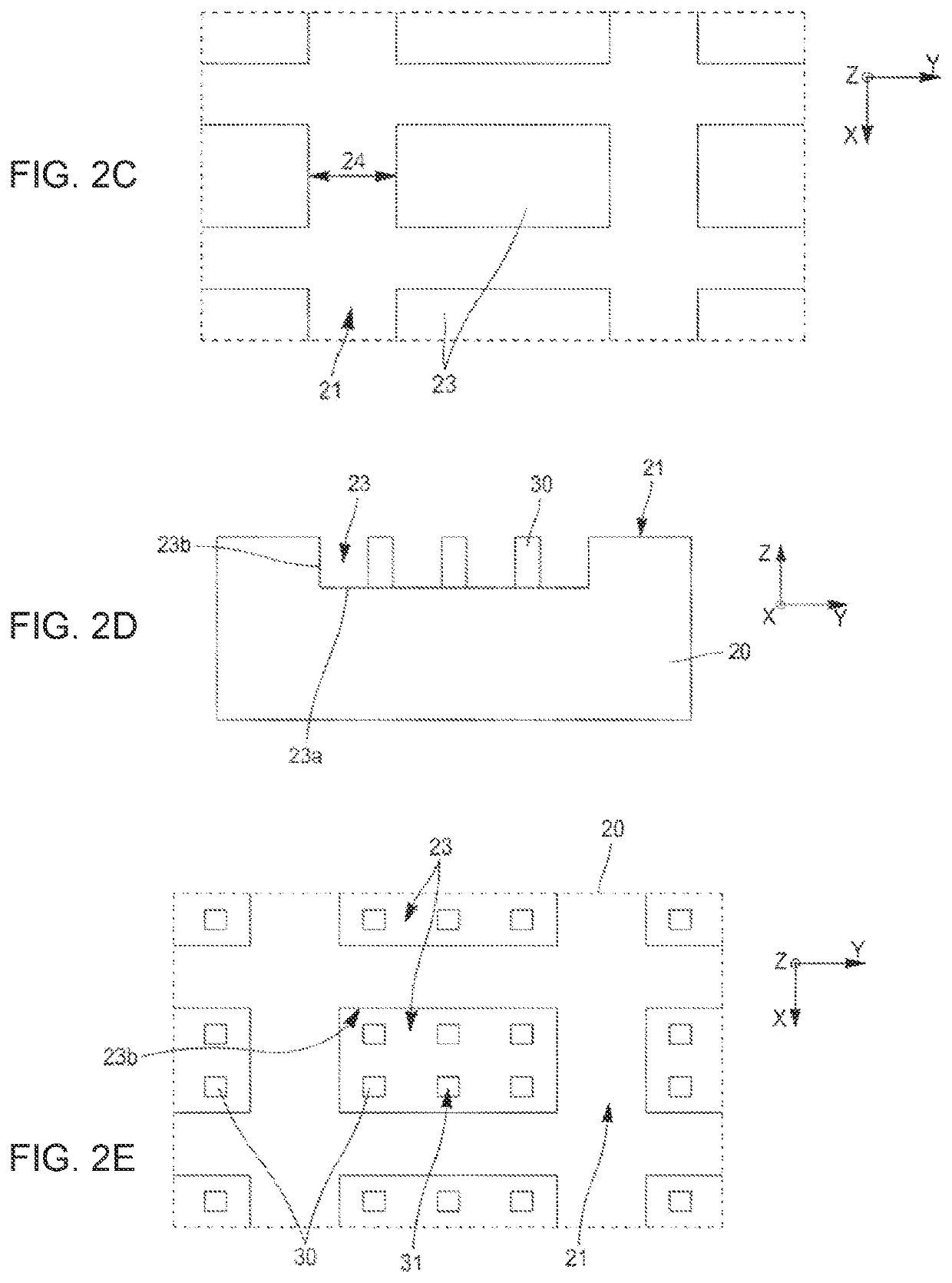
[0093]In the present example, it is sought to form a structure 100 comprising buried cavities 23 comprising a superficial layer made of silicon of 1.5 microns thickness and cavities of 250 microns side length, 0.5 micron depth and spaced apart by 100 microns.
[0094]The donor substrate 1 is a substrate made of silicon (FIG. 5A). An oxide layer 5, for example, of about 50 nm thickness, is formed, for example, by thermal oxidation, on the front side 11 thereof prior to the implantation of the light species. The implantation energy is set to 210 keV, with hydrogen species at a dose of about 7E16 / cm2. Thus, a buried fragile region 2, lying between a first portion 3 and a second portion 4 of the donor substrate 1, is formed.
[0095]The oxide layer 5 will possibly be preserved or removed prior to the step of joining to the carrier substrate 20.
[0096]The carrier substrate 20 is a substrate made of silicon. A thermal-oxide layer 26 having a thickness of 0.5 micron is formed on the carrier subst...
PUM
| Property | Measurement | Unit |
|---|---|---|
| Thickness | aaaaa | aaaaa |
| Thickness | aaaaa | aaaaa |
| Area | aaaaa | aaaaa |
Abstract
Description
Claims
Application Information