Probe assembly

a technology of probe assembly and probe body, which is applied in the direction of electrical testing, measurement devices, instruments, etc., can solve the problems of no design scheme for the probe based on an ss architecture in the prior, and the foregoing probe structure including grounding probes cannot be used, so as to reduce the effective bandwidth of the probe assembly

Active Publication Date: 2022-03-10
MICROELECTRONICS TECH INC
View PDF9 Cites 0 Cited by
  • Summary
  • Abstract
  • Description
  • Claims
  • Application Information

AI Technical Summary

Benefits of technology

[0007]One of the features of the present invention is including no grounding probe, thereby being applied to a to-be-tested device of which test contacts include no grounding point. Another feature of the present invention is that the grounding layers (metal layers) on both sides of the pogo pin are reduced, so that during the test, a test signal will not be coupled to the grounding layers on both sides and generate a radiation resonance to reduce an effective bandwidth of the probe assembly.

Problems solved by technology

Accompanied with more compact and diversified wiring and layout design of a printed circuit board, a form in which test contacts of a to-be-tested object include no grounding point may come out in the future, resulting in that the foregoing probe structure including grounding probes cannot be used.
In other words, there is no design scheme for the probe based on an SS architecture in the prior art.

Method used


Image

  • Probe assembly
  • Probe assembly
  • Probe assembly

Examples


first embodiment

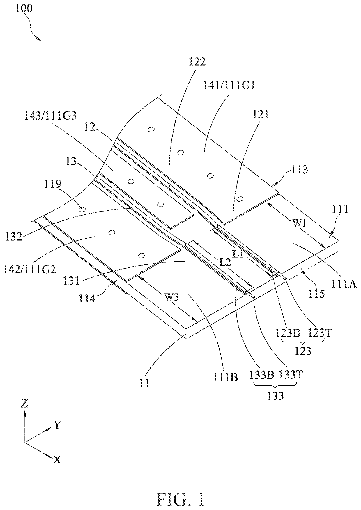
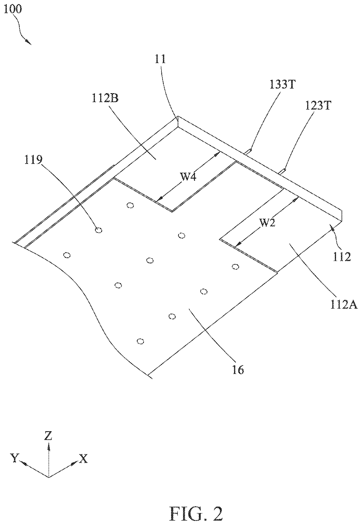
[0021]FIG. 1 and FIG. 2 are respectively a schematic perspective view (I) and a schematic perspective view (II) according to the present invention, which illustrate a probe assembly 100. The probe assembly 100 includes a dielectric layer 11, a first signal line 12, a second signal line 13, a first pogo pin 123, a second pogo pin 133, a first upper grounding layer 141, a second upper grounding layer 142, and a lower grounding layer 16. The probe assembly 100 is applicable to perform a differential signal test on high-speed signal transmission lines of a printed circuit board, and is particularly applicable to a printed circuit board of which test contacts include no grounding point.

[0022]The dielectric layer 11 includes an upper surface 111, a lower surface 112, a first side 113, a second side 114, and a third side 115, where the first side 113 and the second side 114 are opposite to each other, the third side 115 is located between the first side 113 and the second side 114. The upp...

third embodiment

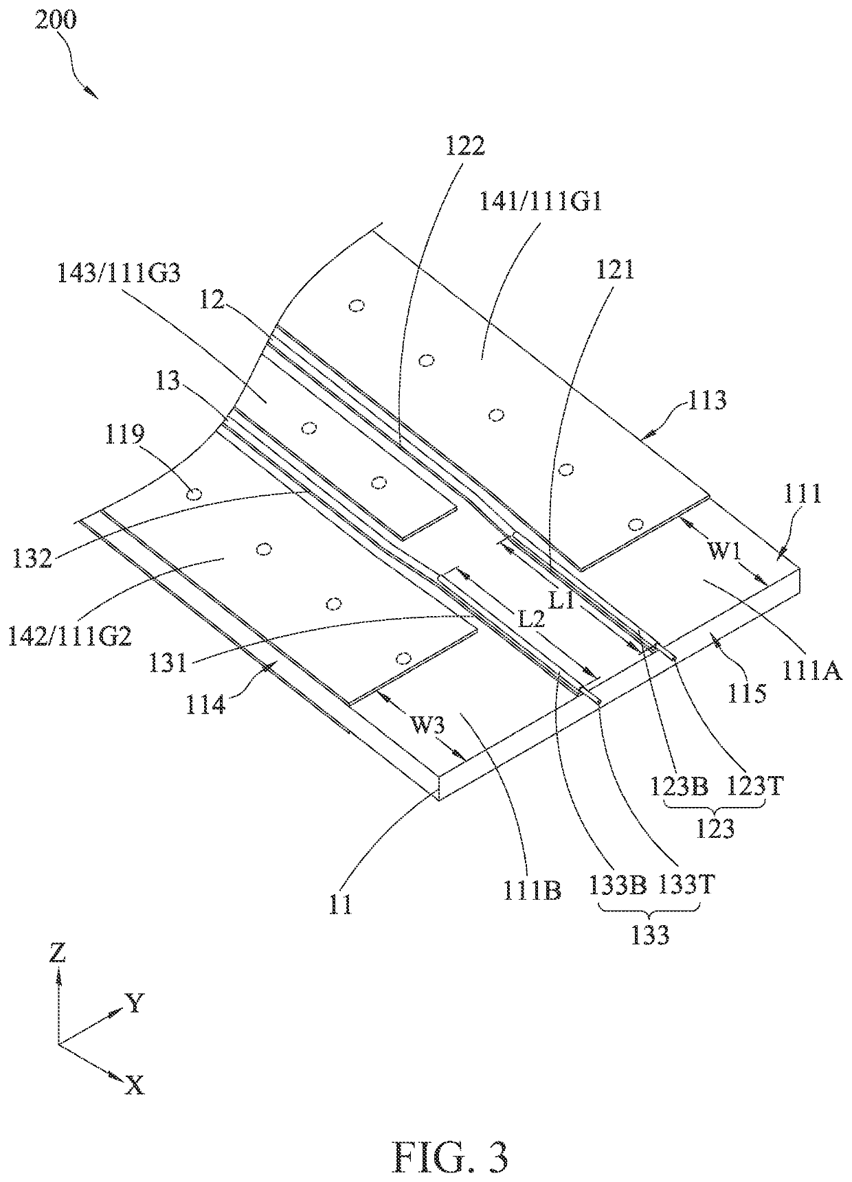
[0034]FIG. 5 and FIG. 6 are respectively a schematic perspective view (I) and a schematic perspective view (II) according to the present invention, which illustrate a probe assembly 300. The probe assembly 300 includes a dielectric layer 21, a first signal line 22, a second signal line 23, a first pogo pin 223, a second pogo pin 233, an upper grounding layer 24, and lower grounding layer 26. The probe assembly 300 is similarly applied to perform a differential signal test on high-speed signal transmission lines of a printed circuit board, and is particularly applied to a printed circuit board of which test contacts include no grounding point.

[0035]As shown in the figure, the dielectric layer 21 includes an upper surface 211, a lower surface 212, and the dielectric layer 21 may be divided into a body portion 21A and a protruding portion 21B. The body portion 21A includes a side 215. The protruding portion 21B extends and protrudes from the side 215 of the body portion 21A in the firs...


PUM


Abstract

A probe assembly, adapted to test high-speed signal transmission lines of printed circuit boards, includes two pogo pins for providing high-frequency differential test signals, and both sides of the pogo pin include no metal layer (grounding layer). Experiments have found that when the two pogo pins test a to-be-tested object, the test signal will be coupled to the metal layers on both sides of the pogo pins to generate a radiation resonance, resulting in a loss of the test signal on a specific frequency band, and further reducing the effective bandwidth of the probe assembly. The metal layers on both sides of the pogo pins of the probe assembly are reduced, so that the foregoing radiation resonance phenomenon can be avoided.

Description

CROSS-REFERENCE TO RELATED APPLICATION[0001]This non-provisional application claims priority under 35 U.S.C. § 119(a) to Patent Application No. 109131000 in Taiwan, R.O.C. on Sep. 9, 2020, the entire contents of which are hereby incorporated by reference.BACKGROUNDTechnical Field[0002]The present invention relates to a probe assembly, and in particular, to a probe assembly applied to perform a high-speed differential signal test.Related Art[0003]A conventional probe structure for measuring a differential signal includes multiple probes disposed on a printed circuit board, and probe arrangement manners of the probe structure are GSS, SSG, SGS, GSSG and GSGSG, where G represents a grounding probe, and S represents a signal probe. Accompanied with more compact and diversified wiring and layout design of a printed circuit board, a form in which test contacts of a to-be-tested object include no grounding point may come out in the future, resulting in that the foregoing probe structure in...

Claims


Application Information

Patent Timeline
Patent Type & Authority Applications(United States)
IPC IPC(8): G01R1/067
CPCG01R1/06722G01R1/06761G01R1/0735
Inventor HSIEH, MING-HSIANGCHOU, CHIA-NANWEI, HAOLIU, CHIA-JUNGYU, CHIA-AN
Owner MICROELECTRONICS TECH INC
Why Eureka
Try Eureka