Radiation detection element, radiation detector and radiation detection device

a radiation detection element and detector technology, applied in the direction of radiation intensity measurement, instruments, x/gamma/cosmic radiation measurement, etc., can solve the problems of increasing size and complicating structure, and achieve the effect of increasing the size of the radiation detection element and improving the radiation detection efficiency

Pending Publication Date: 2022-03-24
HORIBA LTD
View PDF1 Cites 0 Cited by
  • Summary
  • Abstract
  • Description
  • Claims
  • Application Information

AI Technical Summary

Benefits of technology

[0028]In the present invention, the range capable of collecting charges generated by radiation to the first electrode is expanded, so that a sensitive area capable of detecting radiation in the radiation detection element is expanded. The present invention has a remarkable effect that is improvement in the detection efficiency of radiation or prevention of increase in size of the radiation detection element.

Problems solved by technology

The radiation detection element provided with an electrode for increasing the electric potential gradient further needs a structure to place wiring or the like to apply a potential to the electrode, which complicates the structure and increases the size.

Method used


Image

  • Radiation detection element, radiation detector and radiation detection device
  • Radiation detection element, radiation detector and radiation detection device
  • Radiation detection element, radiation detector and radiation detection device

Examples


embodiment 1

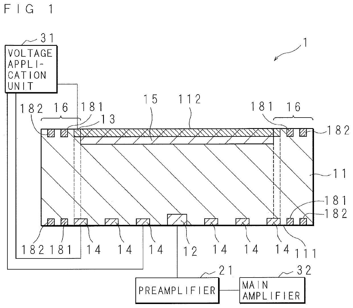
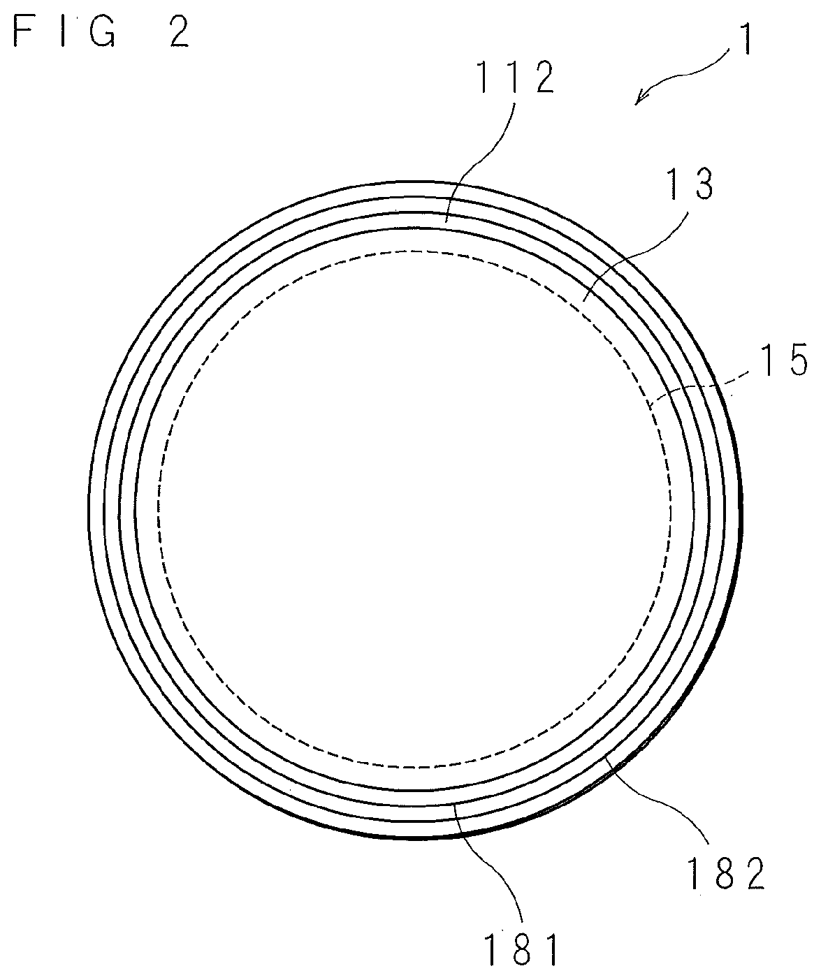
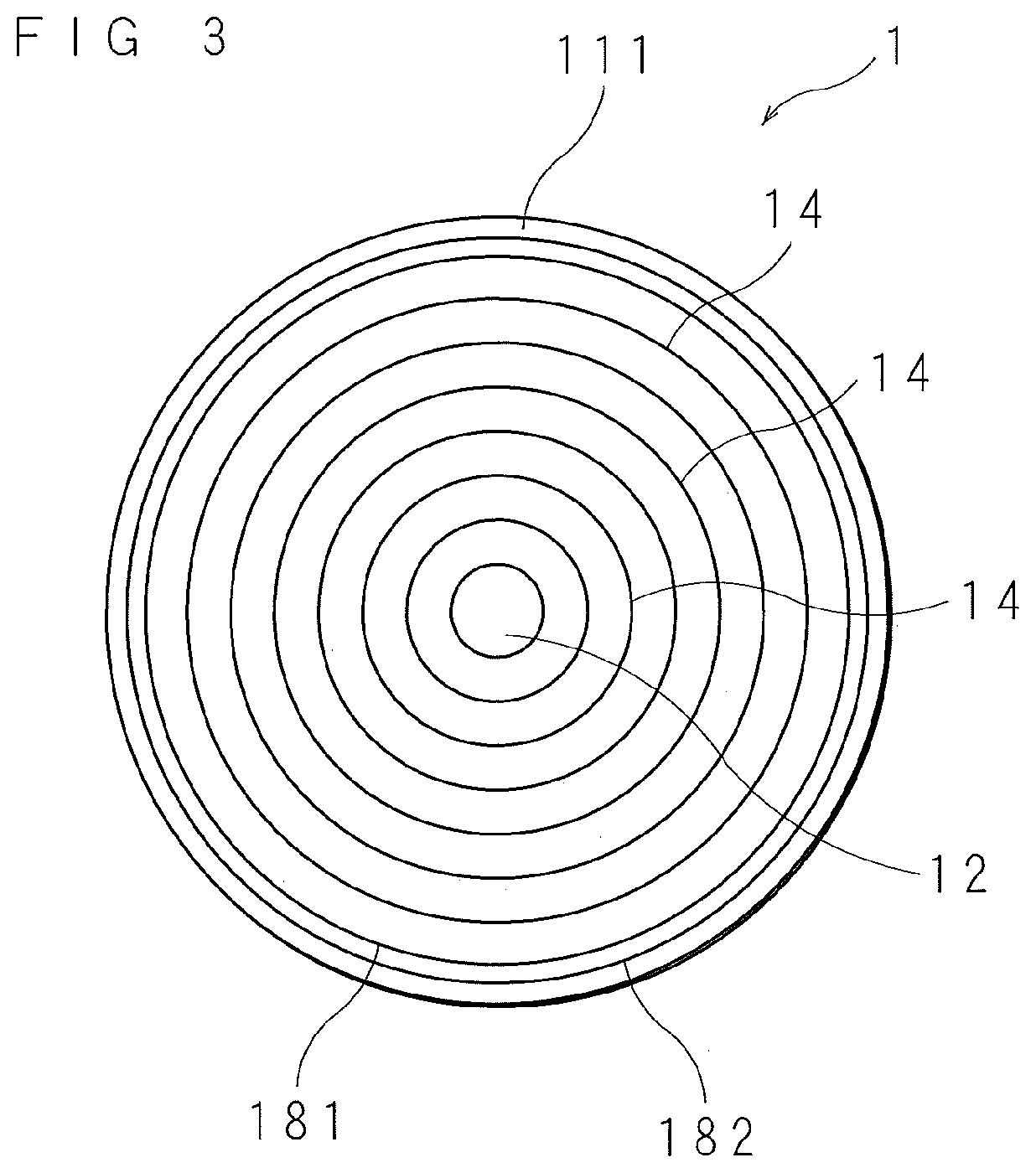
[0042]FIG. 1 is a schematic cross-sectional view of a radiation detection element 1 according to Embodiment 1. The radiation detection element 1 is a silicon drift detection element. The radiation detection element 1 is provided with a Si layer 11 made of silicon (Si) having a discoid shape. The constituent of the Si layer 11 is an n-type Si. The Si layer 11 is a semiconductor part. The Si layer 11 has a first surface 111 and a second surface 112 located on the reverse side of the first surface 111. The second surface 112 is an incident surface on which radiation is mainly incident. FIG. 2 is a schematic plan view of the radiation detection element 1 according to Embodiment 1 when viewed from the second surface 2 side. FIG. 3 is a schematic plan view of the radiation detection element 1 according to Embodiment 1 when viewed from the first surface 111 side.

[0043]At the center of the first surface 111, a signal output electrode 12 is disposed for outputting a signal when radiation is ...

embodiment 2

[0066]FIG. 10 is a schematic plan view of the radiation detection element 1 according to Embodiment 2 when viewed from the first surface side 111. Multiple sets of multiple curved electrodes 14 each having a ring shape are disposed on the first surface 111 of the Si layer 11. FIG. 10 shows an example in which four sets of multiple curved electrodes 14 are disposed. Any number of sets of the multiple curved electrodes such as eight sets or the like is appropriate without being limited to four sets. The multiple sets of the multiple curved electrodes 14 are arranged evenly around the center of the first surface 111. Though FIG. 10 shows an example in which three curved electrodes 14 are included in each set, more curved electrodes 14 are disposed in practice. At the position surrounded by the multiple curved electrodes 14 of each set, a signal output electrode 12 is disposed. The outermost curved electrodes 14 included in the respective sets of the multiple curved electrodes 14 are pa...


PUM

PropertyMeasurementUnit
distanceaaaaaaaaaa
distanceaaaaaaaaaa
voltageaaaaaaaaaa

Abstract

The radiation detection element comprising a semiconductor part having a plate shape, a first electrode that is disposed on a first surface being one surface of the semiconductor part and that collects charges generated by incidence of radiation in the semiconductor part, a second electrode that is disposed on a second surface being the other surface of the semiconductor part and that is applied with voltage needed for collecting the charges, and a heavily-doped layer that is disposed at a region of the second surface excluding an edge of the semiconductor part and is doped heavier than the semiconductor part with dopants for making a type of a semiconductor equal to that of the semiconductor part. The heavily-doped layer is on the second surface located at a position overlapped with the second electrode and is thicker than the second electrode.

Description

TECHNICAL FIELD[0001]The present invention relates to a radiation detection element, a radiation detector and a radiation detection device.BACKGROUND ART[0002]Examples of a radiation detector for detecting radiation such as X-rays or the like include a radiation detection element with a semiconductor. Examples of the radiation detection element with a semiconductor include a silicon drift detection element, for example. A radiation detector provided with the silicon drift detection element is called a silicon drift detector (SDD).[0003]The radiation detection element with a semiconductor includes a flat-plate semiconductor part. The semiconductor part has a first electrode that outputs a signal on one surface and a second electrode that is applied with voltage on the other surface. By application of voltage, an electric field is generated inside the semiconductor part. If radiation is incident into the semiconductor part, electric charges are generated inside the semiconductor part ...

Claims


Application Information

Patent Timeline
Patent Type & Authority Applications(United States)
IPC IPC(8): H01L31/115H01L31/0203
CPCH01L31/115H01L31/0203G01T1/24G01T1/2928
Inventor MATSUNAGA, DAISUKEPICCIOTTO, ANTONINOBORGHI, GIACOMO
Owner HORIBA LTD
Why Eureka
Try Eureka