Touch panel, manufacturing method of touch panel, and device thereof

Inactive Publication Date: 2022-03-31
TPK ADVANCED SOLUTIONS
View PDF0 Cites 0 Cited by
  • Summary
  • Abstract
  • Description
  • Claims
  • Application Information

AI Technical Summary

Benefits of technology

[0029]According to the aforementioned embodiments of the present disclosure, since the peripheral trace located on the peripheral area and the touch sensing electrode located on the visible area in the touch panel of the present disclosure are both formed of the modified metal nanowires, the surface resistance of the touch panel can be effectively reduced to enhance the conductivity of the touch panel, and the resistive capacitive loading value of the touch panel can be reduced. On the other hand, since the touch sensing electrode on the visible area has the mesh pattern interlaced by multiple thin lines, the touch sensing electrode can prevent the light transmittance of the visible area from being affected by the modified metal nanowires. As a result, the visible area of the touch p

Problems solved by technology

However, these metal oxide films cannot meet the flexibility requirements of display devices.
However, there are still many problems for the process technology of the aforementioned nano-scale materials to be solved.
For example, when using nanowires to manufacture touch electrodes, the touch electrodes must be connected to the traces made of metal in the peripheral area, and the overlapping area where the touch electrode an

Method used


Image

  • Touch panel, manufacturing method of touch panel, and device thereof
  • Touch panel, manufacturing method of touch panel, and device thereof
  • Touch panel, manufacturing method of touch panel, and device thereof

Examples


Embodiment Construction

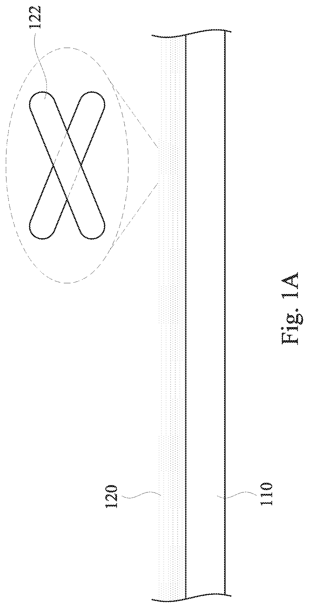
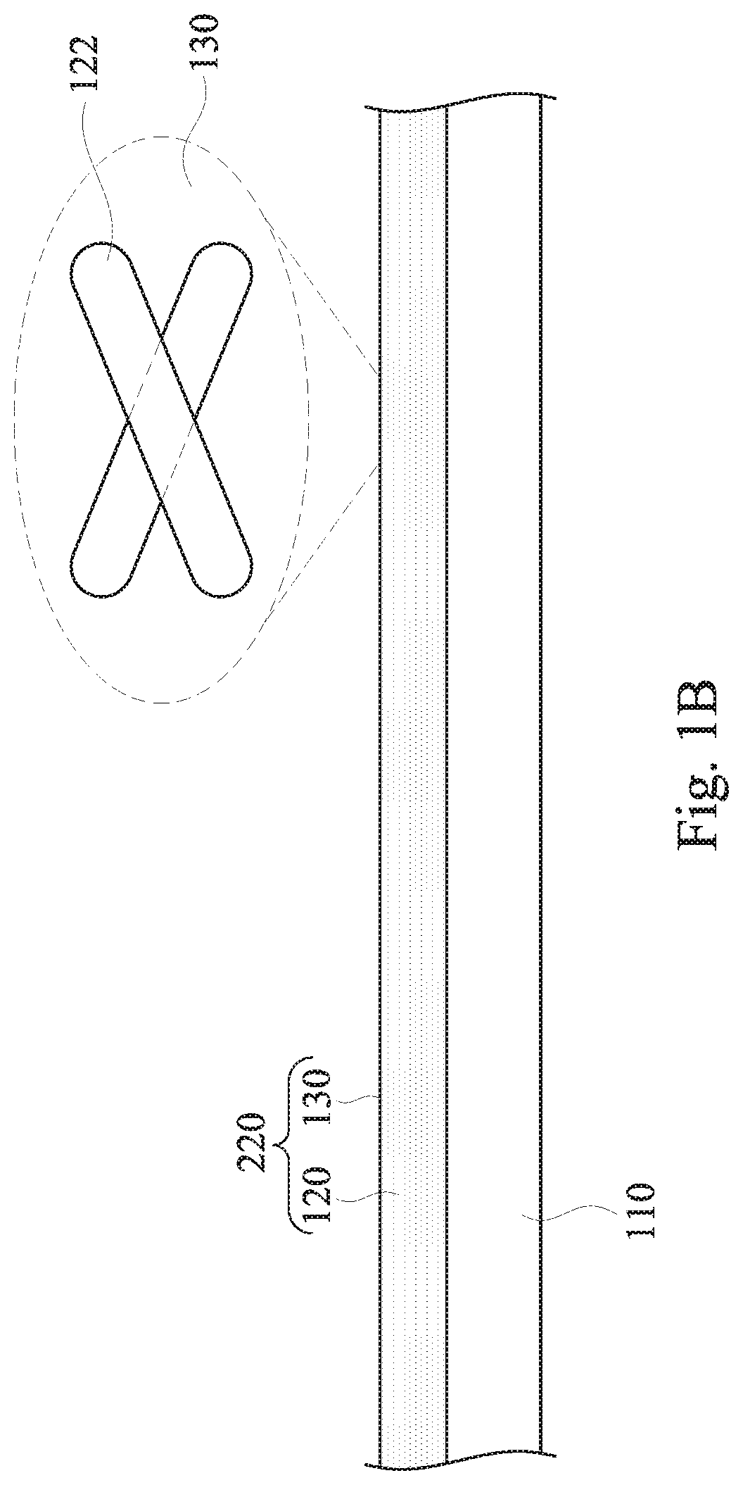
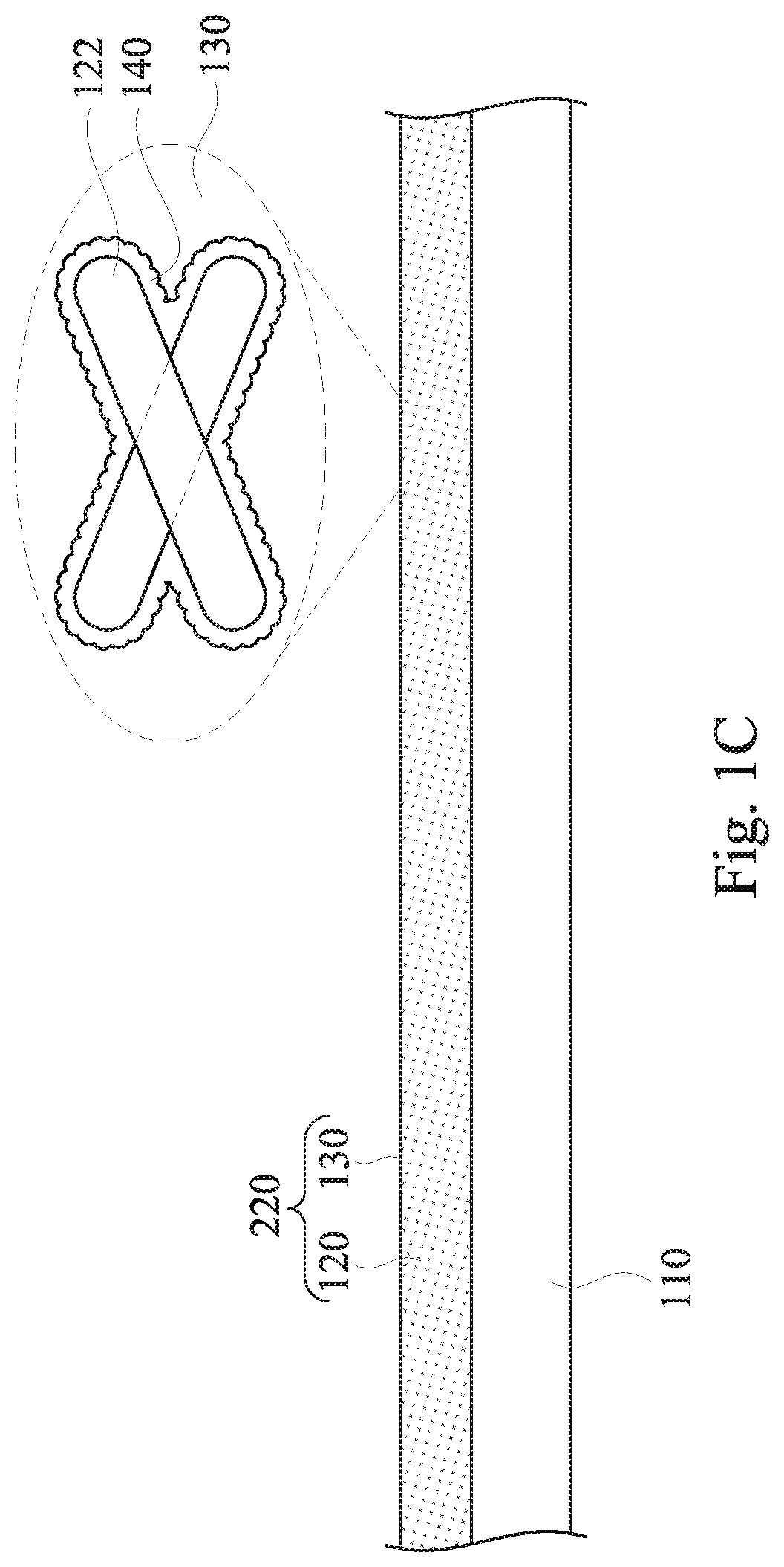
[0038]Reference will now be made in detail to the present embodiments of the disclosure, examples of which are illustrated in the accompanying drawings. Wherever possible, the same reference numbers are used in the drawings and the description to refer to the same or like parts.

[0039]In addition, relative terms such as “lower” or “bottom” and “upper” or “top” can be used herein to describe the relationship between one element and another element, as shown in the figure. It should be understood that relative terms are intended to include different orientations of the device other than those shown in the figures. For example, if the device in one figure is turned over, elements described as being on the “lower” side of other elements will be oriented on the “upper” side of the other elements. Therefore, the exemplary term “lower” may include an orientation of “lower” and “upper”, depending on the specific orientation of the drawing. Similarly, if the device in one figure is turned ove...


PUM


Abstract

A touch panel includes a substrate, a peripheral trace, and a touch sensing electrode. The substrate has a visible area and a peripheral area. The peripheral trace is disposed on the peripheral area of the substrate. The touch sensing electrode is disposed on the visible area of the substrate, is electrically connected to the peripheral trace, and has a mesh pattern interlaced by a plurality of thin lines. The peripheral trace and the touch sensing electrode each includes a plurality of conductive nanostructures and a film layer added onto the conductive nanostructures, and an interface between the conductive nanostructures and the film layer substantially has a covering structure.

Description

BACKGROUNDField of Disclosure[0001]The present disclosure relates to a touch panel, a manufacturing method of the touch panel, and a device including the aforementioned touch panel.Description of Related Art[0002]In recent years, transparent conductors are often applied to many display or touch-related devices since transparent conductors can both transmit light and provide appropriate conductivity. In general, the transparent conductor may be a film made of various metal oxides, such as indium tin oxide (ITO) film, indium zinc oxide (IZO) film, cadmium tin oxide (CTO) film, or aluminum-doped zinc oxide (AZO) film. However, these metal oxide films cannot meet the flexibility requirements of display devices. Therefore, a variety of flexible transparent conductors have been developed, for example, a transparent conductor made of nano-scale materials.[0003]However, there are still many problems for the process technology of the aforementioned nano-scale materials to be solved. For exam...

Claims


Application Information

Patent Timeline
IPC IPC(8): G06F3/044G06F3/041
CPCG06F3/0445G06F2203/04112G06F2203/04103G06F3/0412G06F3/0446G06F3/04164
Inventor YU, CHIEN-HSIENDING, ZI JUNLAI, YI YUNKE, YONG BINFANG, QIN XUE
Owner TPK ADVANCED SOLUTIONS
Why Eureka
Try Eureka