
Multi-layer PCB stack for color mixing

Pending Publication Date: 2022-04-28
SIGNIFY HLDG BV
View PDF0 Cites 0 Cited by
  • Summary
  • Abstract
  • Description
  • Claims
  • Application Information

AI Technical Summary

Benefits of technology

The patent describes a lighting device that can be produced easily and uses a high density of light sources. The device can control the color and temperature of the light, which makes it more versatile than other solutions. The device consists of a printed circuit board (PCB) with conductive tracks, pads, and other features etched from layers of copper. The PCB also has a coating to protect the copper from corrosion. Overall, the device provides a simple and effective way to control the lighting.

Problems solved by technology

This may mean that part of the available space in the LES cannot be used for a lighting element.
When a multi-color architecture with e.g. red, green, blue and white LEDs is composed, the related routing will be much more complicated and may occupy a great deal of the available space to connect all different colors individually.
It may be unavoidable that the routing may have to be placed in between adjacent LEDs which may enlarge the LED to LED distance substantially, and with that the LES of the complete architecture.
Thereby, undesirably the etendue may be increased.
In this case, the routing may occupy more space than needed for a LED itself and therefor a great benefit of using e.g. mini-LEDs may be lost.
This may require a substantial amount of vias to connect all layers electrically.
The extensive routing may consume a lot of space needed for thermal dissipation of the generated heat by the LEDs.

Method used


Image

  • Multi-layer PCB stack for color mixing
  • Multi-layer PCB stack for color mixing
  • Multi-layer PCB stack for color mixing

Examples


Embodiment Construction

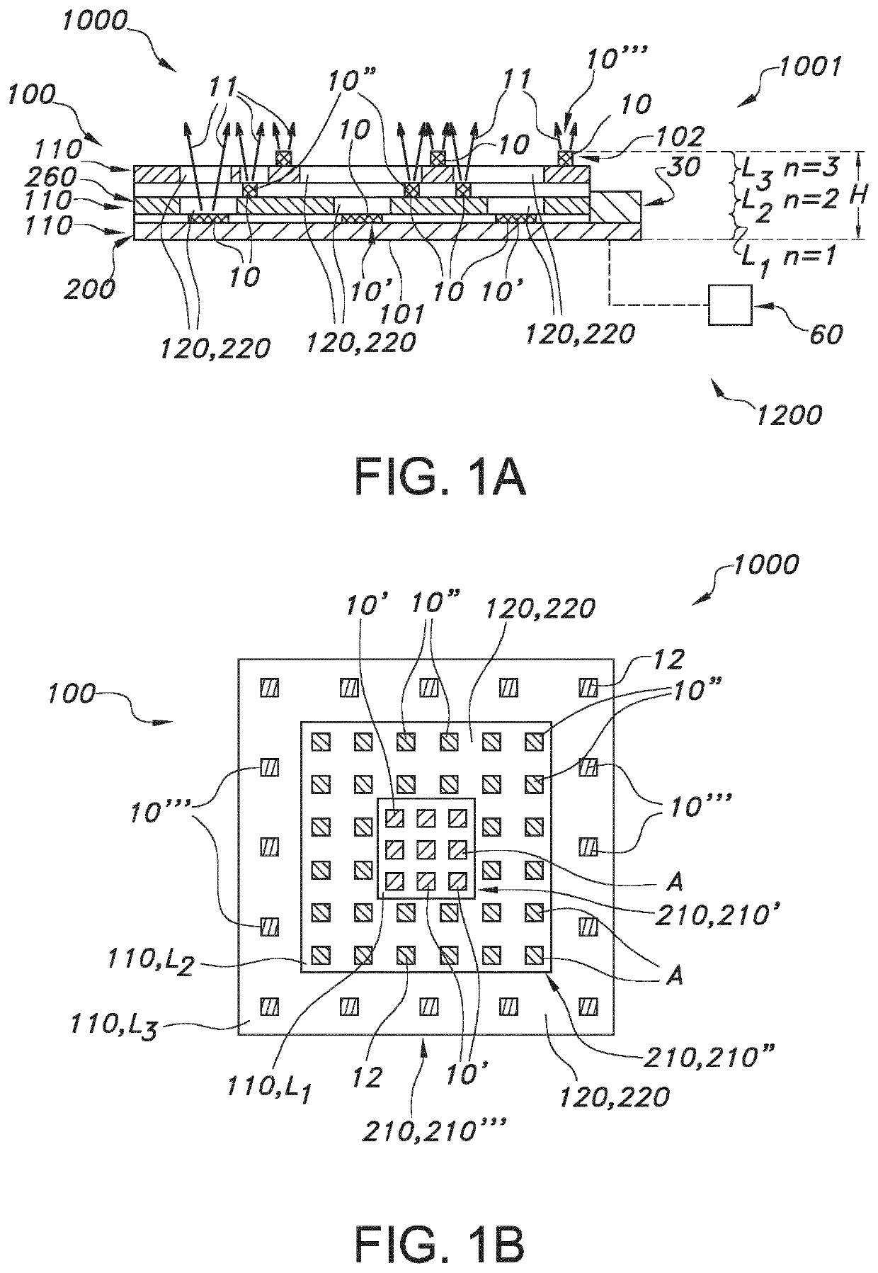
[0074]FIG. 1a schematically depicts—in a cross-sectional view—an embodiment of a lighting device 1000 comprising a multi-layer PCB stack 100 comprising n stacked layers 110, wherein n≥2. Here, by way of example n=3. Further, k layers 110 of the n stacked layers 110 each comprises a PCB 200 with a solid state light source 10, wherein 2≤k≤n. Here, k is also 3. Note that k is not necessarily n, but k is especially at least 2. Three layers 110 (or levels) are depicted, indicated with references L1, L2, and L3. The solid state light sources 10 are configured to generate light source light 11.

[0075]The layers 110 are shaped and stacked such that the light source light 11 of a light source 10 of any of the PCBs 200 is at least partly not physically blocked by any of the other PCBs 200. Hence, a kind of pyramid like structures are provided, with in embodiments at the steps solid state light sources.

[0076]As schematically depicted PCBs 200 of higher numbered layers 110 do not physically bloc...


PUM


Abstract

The invention provides a lighting device (1000) comprising a multi-layer PCB stack (100) comprising n stacked layers (110), wherein n≥2, wherein k layers (110) of the n stacked layers (110) each comprises a PCB (200) with a solid state light source (10), wherein 2≤k≤n, wherein the solid state light sources (10) are configured to generate light source light (11), wherein the layers (110) are shaped and stacked such that the light source light (11) of a 5 light source (10) of any of the PCBs (200) is at least partly not physically blocked by any of the other PCBs (200).

Description

FIELD OF THE INVENTION[0001]The invention relates to a lighting device, a luminaire comprising such lighting device, and to a lighting system comprising such lighting device. The invention also relates to a method of providing such lighting device.BACKGROUND OF THE INVENTION[0002]RGB-stack light emitting diode modules are known in the art. A paper by Ying-Chang Li et al. titled RGB-Stack Light Emitting Diode Modules with Transparent Glass Circuit Board and Oil Encapsulation, Materials 2018, vol. 11, 65 (2018 Materials (Basel). March 1; 11(3). pii: E365. doi: 10.3390 / ma11030365) indicates that the “light emitting diode (LED) is widely used in modern solid-state lighting applications, and its output efficiency is closely related to the submounts' material properties. Most submounts used today, such as low-power printed circuit boards (PCBs) or high-power metal core printed circuit boards (MCPCBs), are not transparent and seriously decrease the output light extraction. To meet the requ...

Claims


Application Information

Patent Timeline
IPC IPC(8): H01L33/62H01L25/075H01L33/50H05B44/00
CPCH01L33/62H01L33/505H01L25/0756H01L33/50H05B45/00
Inventor VAN DER LUBBE, MARCELLUS JACOBUS JOHANNESTER WEEME, BEREND JAN WILLEM
Owner SIGNIFY HLDG BV
Learn More