Micro LED display and repair method thereof

a micro led display and repair method technology, applied in the field of display and a repair method of the micro led display, can solve the problems of display quality decline, broken spot, and weak bonding between the circui

Active Publication Date: 2022-05-12
PLAYNITRIDE DISPLAY CO LTD
View PDF5 Cites 0 Cited by
  • Summary
  • Abstract
  • Description
  • Claims
  • Application Information

AI Technical Summary

Benefits of technology

[0006]An aspect of the disclosure provid

Problems solved by technology

Some of the micro LEDs transferred onto the display substrate may be damaged or misaligned and unable to emit light and thus form a broken spot.
As a result, the display quality may decline.
Since the second soldering layer undergoes at least two reflow processes

Method used


Image

  • Micro LED display and repair method thereof
  • Micro LED display and repair method thereof
  • Micro LED display and repair method thereof

Examples


Embodiment Construction

[0030]Reference will now be made in detail to the present preferred embodiments of the invention, examples of which are illustrated in the accompanying drawings. Wherever possible, the same reference numbers are used in the drawings and the description to refer to the same or like parts.

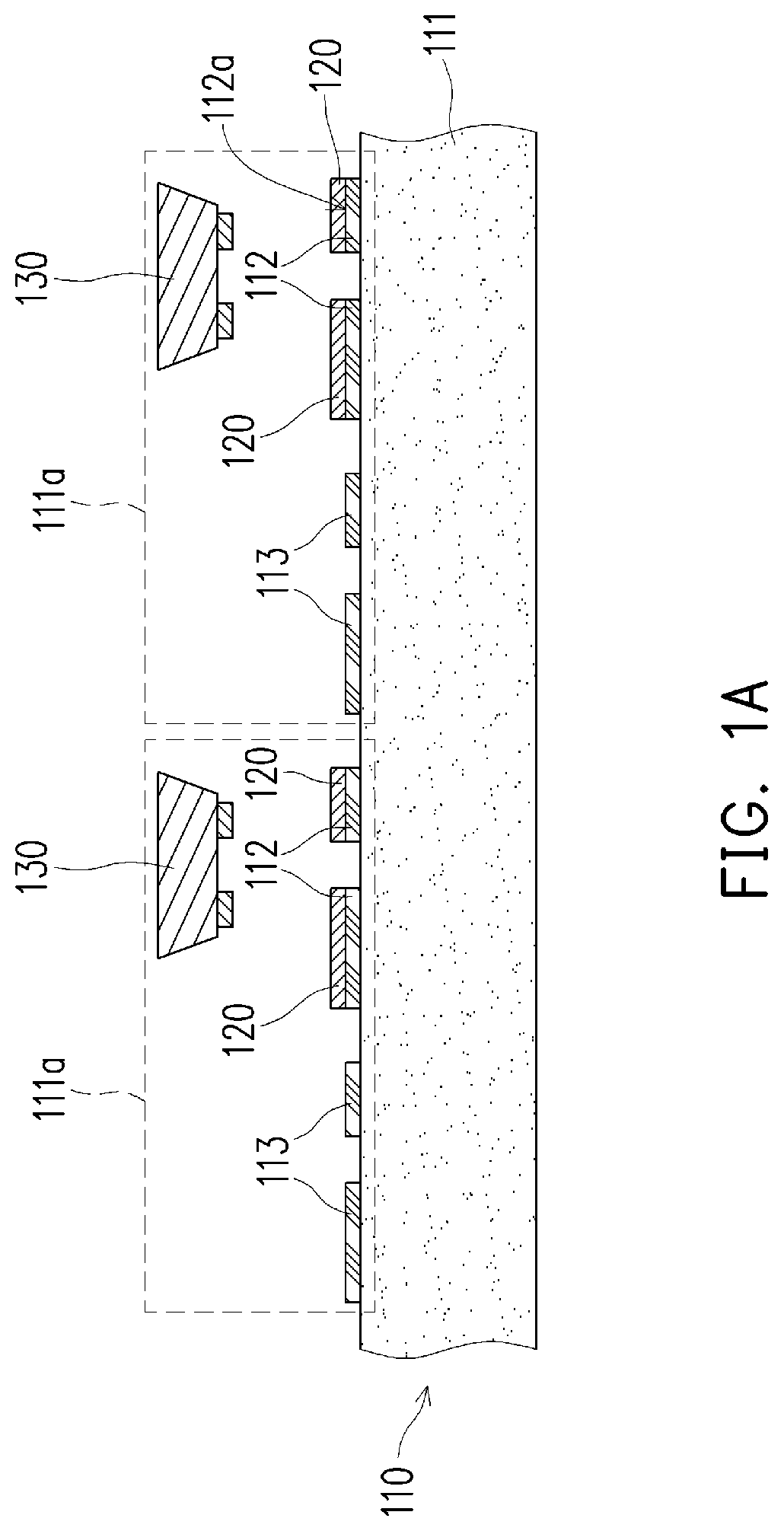
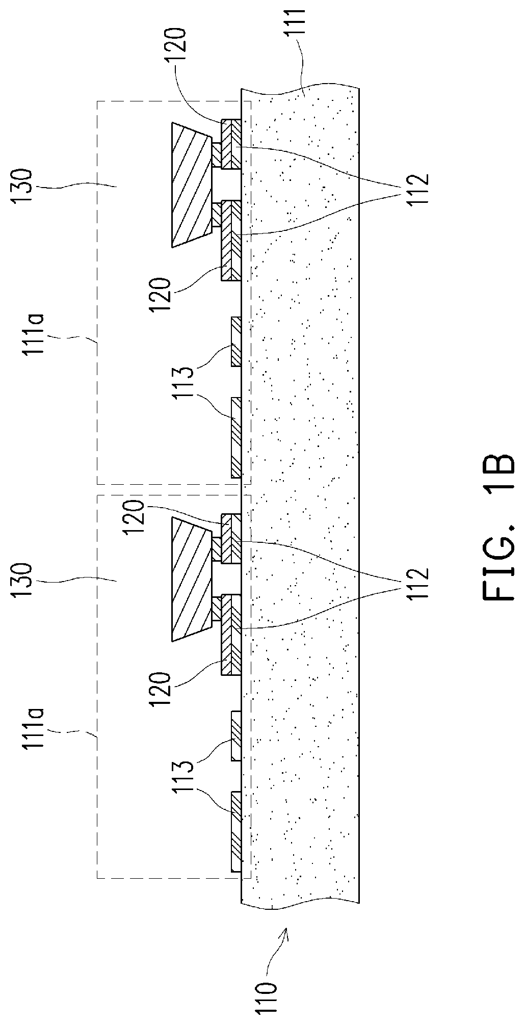
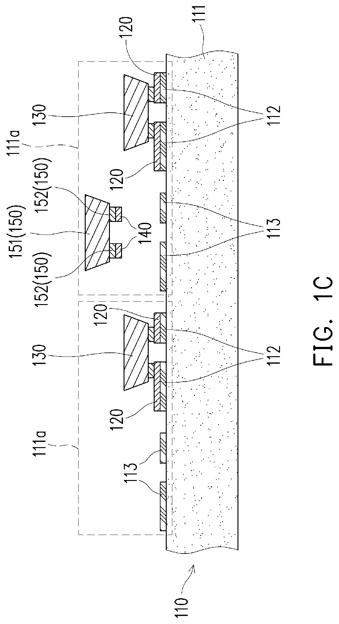
[0031]FIGS. 1A to 1D are schematic partial cross-sectional views of a repair method of a micro LED display according to an embodiment of the disclosure. First, referring to FIG. 1A and FIG. 1B, a transfer procedure is performed. As shown in FIG. 1A, a display substrate 110 is provided. The display substrate 110 includes a substrate 111, a first circuit layer 112 formed on the substrate 111 and a second circuit layer 113 formed on the substrate 111. In addition, the substrate 111 includes multiple pixel areas 111a. In addition, the first circuit layer 112 and the second circuit layer 113 are arranged in each of the pixel areas 111a, and the second circuit layer 113 in each of the pixel areas 111a is d...


PUM


Abstract

A micro LED display includes a display substrate, a first soldering layer, at least one second soldering layer, first micro LEDs and at least one second micro LED. The display substrate includes a substrate having a plurality of pixel areas, a first circuit layer and a second circuit layer, and the first circuit layer and the second circuit layer are arranged in each pixel area. The first soldering layer is disposed on the first circuit layer, and the second soldering layer is disposed on the second micro LED. An arranging area of the first soldering layer is greater than an arranging area of the second soldering layer. The first micro LEDs is bonding to the first circuit layer in each pixel area through the first soldering layer. The second micro LED is bonding to the second circuit layer of one of the pixel areas through the second soldering layer.

Description

CROSS-REFERENCE TO RELATED APPLICATION[0001]This application claims the priority benefit of Taiwan application serial no. 109139461, filed on Nov. 12, 2020. The entirety of the above-mentioned patent application is hereby incorporated by reference herein and made a part of this specification.BACKGROUNDTechnical Field[0002]The disclosure relates to a display and a repair method of the display, in particular, to a micro LED display and a repair method of the micro LED display.Description of Related Art[0003]With the development of display technologies, backlights in displays have evolved from LED backlights to mini LED backlights or micro LED backlights. Taking micro LED backlights for example, millions or tens of millions of micro LEDs are transferred from an epitaxial substrate to a display substrate through mass transfer. Some of the micro LEDs transferred onto the display substrate may be damaged or misaligned and unable to emit light and thus form a broken spot. As a result, the ...

Claims


Application Information

Patent Timeline
IPC IPC(8): H01L27/15H01L33/48H01L33/62G09G3/00H01L33/38
CPCH01L27/156H01L33/486H01L33/382G09G3/006H01L33/62H01L25/0753H01L33/0095H01L22/30G01R31/2635
Inventor TANG, HSIANG-WENLAI, YU-HUNG
Owner PLAYNITRIDE DISPLAY CO LTD
Why Eureka
Try Eureka