Method for repairing disconnecting signal line of thin film transistor (TFT) array substrate

a technology of array substrates and thin films, applied in the field of display technology, can solve the problems of line defects, affecting product yield and production costs, and difficult control of processes, and achieve the effect of improving the repairing yield and improving the repairing effect of the disconnecting signal lin

Active Publication Date: 2020-06-16
SHENZHEN CHINA STAR OPTOELECTRONICS SEMICON DISPLAY TECH CO LTD
View PDF5 Cites 0 Cited by
  • Summary
  • Abstract
  • Description
  • Claims
  • Application Information

AI Technical Summary

Benefits of technology

[0007]The present application provides a method for repairing a disconnecting signal line of a thin film transistor (TFT) array substrate for improving a method for repairing a disconnecting signal line of the large-scale OLED display panel, to solve the present method for repairing the disconnecting signal line of the TFT array substrate, during melting the signal lines and the repairing lines by a laser process, the exceeding melting will cause the whole area pierced, the insufficient melting will be not able to connect the repairing lines to the signal lines to affect the disconnecting signal line repairing effect, further to impact on the display effect of the display screen.
[0023]The advantages of the present application are: in the method for repairing the disconnecting signal line of the TFT array substrate, the insulating layer placed at edge of the disconnecting signal lines is melted, and filled with the solidified metal nanoparticles to realize a connection between the disconnecting signal line and the repairing lines and to improve a repairing effect of the disconnecting signal line and to improve a repairing yield.

Problems solved by technology

In the present AMOLED (Active Matrix Organic Light Emitting Diode) display, signal lines are mainly used to provide video signals to drive pixel circuits, but during the manufacturing process, due to affected by up and down fluctuations, environmental particles, etching processes, etc. of the substrate surface, disconnecting signal lines are easy occurred in the signal lines, to lead a number of line defects.
Moreover, as a size of the AMOLED panel increased and the resolution increased, a number of signal lines are designed, a narrower line width is requested, it is a more difficult process and more chance to cause a disconnecting signal line, and ultimately a product yield and production costs are impacted.
However, it is difficult to control a process of melting the insulating layer formed between the signal lines and the repairing lines to make them to be connected by the laser process, a exceeding melting will cause a whole area pierced, an insufficient melting will be not able to connect the repairing lines to the signal lines, and finally the repairing effect is affected.
Above all, the present the method for repairing the disconnecting signal lines of the TFT array substrate, the signal lines and the repairing lines are melted by a laser process, the exceeding melting will cause the whole area pierced, the insufficient melting will be not able to connect the repairing lines to the signal lines to affect the disconnecting signal line repairing effect, further to impact on the display effect of the display screen.
The present method for repairing the disconnecting signal lines of the TFT array substrate, during melting the signal lines and the repairing lines by a laser process, the exceeding melting will cause the whole area pierced, the insufficient melting will be not able to connect the repairing lines to the signal lines to affect the disconnecting signal line repairing effect, further to impact on the display effect of the display screen.

Method used


Image

  • Method for repairing disconnecting signal line of thin film transistor (TFT) array substrate
  • Method for repairing disconnecting signal line of thin film transistor (TFT) array substrate

Examples


Embodiment Construction

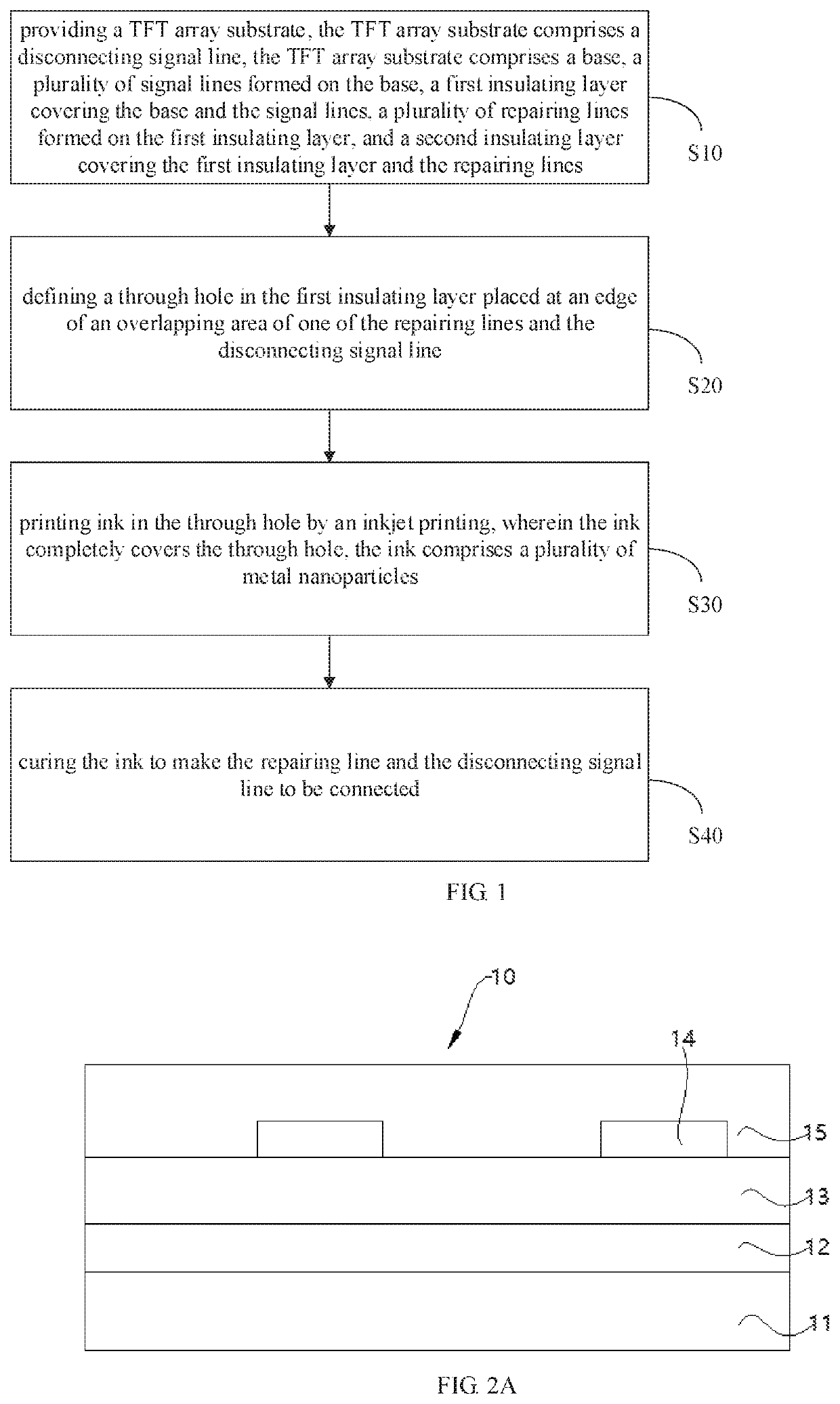
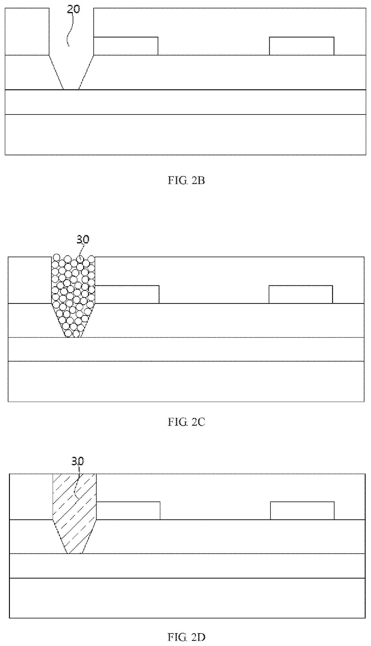
[0027]The description of following embodiment, with reference to the accompanying drawings, is used to exemplify specific embodiments which may be carried out in the present disclosure. Directional terms mentioned in the present disclosure, such as “top”, “bottom”, “front”, “back”, “left”, “right”, “inside”, “outside”, “side”, etc., are only used with reference to the orientation of the accompanying drawings. Therefore, the used directional terms are intended to illustrate, but not to limit, the present disclosure. In the drawings, the components having similar structures are denoted by same numerals.

[0028]The present disclosure is directed to a technology problem of a method for repairing a disconnecting signal line of a TFT array substrate in prior art, during melting the signal lines and the repairing lines by a laser process, the exceeding melting will cause the whole area pierced, the insufficient melting will be not able to connect the repairing lines to the signal lines to af...


PUM

PropertyMeasurementUnit
areaaaaaaaaaaa
thicknessaaaaaaaaaa
sizeaaaaaaaaaa

Abstract

A method for repairing a disconnecting signal line of a thin film transistor (TFT) array substrate including: providing a TFT array substrate with a disconnecting signal line; defining a through hole at an edge of an overlapping area of the repairing line and the disconnecting signal line; printing ink in the through hole, the ink completely covers the through hole, the ink contains a plurality of metal nanoparticles; and curing the ink to make the repairing line and the disconnecting signal line to be connected.

Description

RELATED APPLICATIONS[0001]This application is a National Phase of PCT Patent Application No. PCT / CN2018 / 117577 having International filing date of Nov. 27, 2018, which claims the benefit of priority of Chinese Patent Application No. 201811193754.8 filed on Oct. 15, 2018. The contents of the above applications are all incorporated by reference as if fully set forth herein in their entirety.FIELD AND BACKGROUND OF THE INVENTION[0002]The present invention relates to the field of display technology, and particularly to a method for repairing a disconnecting signal line of a TFT array substrate.[0003]In the present AMOLED (Active Matrix Organic Light Emitting Diode) display, signal lines are mainly used to provide video signals to drive pixel circuits, but during the manufacturing process, due to affected by up and down fluctuations, environmental particles, etching processes, etc. of the substrate surface, disconnecting signal lines are easy occurred in the signal lines, to lead a numbe...

Claims


Application Information

Patent Timeline
Patent Type & Authority Patents(United States)
IPC IPC(8): H01L27/32
CPCH01L27/3276H01L2227/323H01L27/1292H01L21/76892H10K59/12H10K71/236H10K71/861H10K59/131H10K59/1201
Inventor LIU, ZHAOSONG
Owner SHENZHEN CHINA STAR OPTOELECTRONICS SEMICON DISPLAY TECH CO LTD
Why Eureka
Try Eureka