

Repair structure and active device array substrate
a technology of active devices and array substrates, which is applied in the direction of radio frequency controlled devices, instruments, optics, etc., can solve the problems of discomfort for users, defect production in the process of fabricating liquid crystal display panels, and the technique of forming liquid crystal display panels is quite mature, so as to increase the repair yield
- Summary
- Abstract
- Description
- Claims
- Application Information
AI Technical Summary
Benefits of technology
Problems solved by technology
Method used
Image

Examples
Embodiment Construction
[0036]Reference will now be made in detail to the present embodiments of the invention, examples of which are illustrated in the accompanying drawings. Wherever possible, the same reference numbers are used in the drawings and the description to refer to the same or like parts.
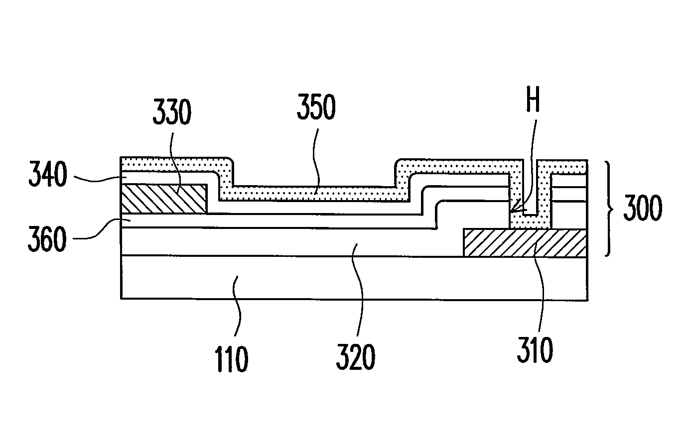
[0037]FIG. 2A is a top view of a repair structure according to one embodiment of the present invention. FIG. 2B is a schematic cross-sectional view along line B-B′ of the repair structure shown in FIG. 2A. As shown in FIGS. 2A and 2B, the repair structure 300 is fabricated over a substrate 110. The repair structure 300 includes a substrate 110, at least one first conducting line 310, a first insulating layer 320, at least one second conducting line 330, a second insulating layer 340 and a repair connecting layer 350. The at least one first conducting line 310 is disposed on the substrate 110. The first insulating layer 320 is disposed over the substrate 110 to cover the first conducting line 310. The second co...
PUM
 Abstract
Description
Claims
Application Information