Method and apparatus for predicting yield of semiconductor devices

a technology for semiconductor devices and yields, applied in the field of process management technology for manufacturing semiconductor devices, can solve the problems of affecting the estimation of chip probing yield, affecting the yield of chip products, and becoming more difficult to put new chip designs into production, so as to accurately predict the defect and yield of semiconductor devices

Pending Publication Date: 2022-06-02
SHANGHAI HUALI INTEGRATED CIRCUIT CORP
View PDF0 Cites 1 Cited by
  • Summary
  • Abstract
  • Description
  • Claims
  • Application Information

AI Technical Summary

Benefits of technology

[0028]The computer-readable storage medium according to the present disclosure stores computer instructions thereon. The computer instructions are executed by the processor to implement the method for predicting the yield of manufacturing semiconductor devices according to any one of the above embodiments, so as to accurately and efficiently predict the defects and yield of the semiconductor devices.

Problems solved by technology

With the increasing complexity of chip design, it is has become more difficult to put new chip designs into production.
Mass data results show that production line defects directly affect the yields of chip products.
However, for some lot wafers that are not reviewed after scanning, or defects on the same wafer that are not sampled for review, the existing production line defect monitoring technology may have the problem of underreporting defects, which will affect the estimation of chip probing yield.
In addition, for some lot wafers with a tight production period or a short Q-Time between two processes, the existing production line defect monitoring technology may directly skip them and scan next lot wafer, or does not scan the defects of these lot wafers, which will affect the estimation of chip probing yield.

Method used


Image

  • Method and apparatus for predicting yield of semiconductor devices
  • Method and apparatus for predicting yield of semiconductor devices
  • Method and apparatus for predicting yield of semiconductor devices

Examples


Embodiment Construction

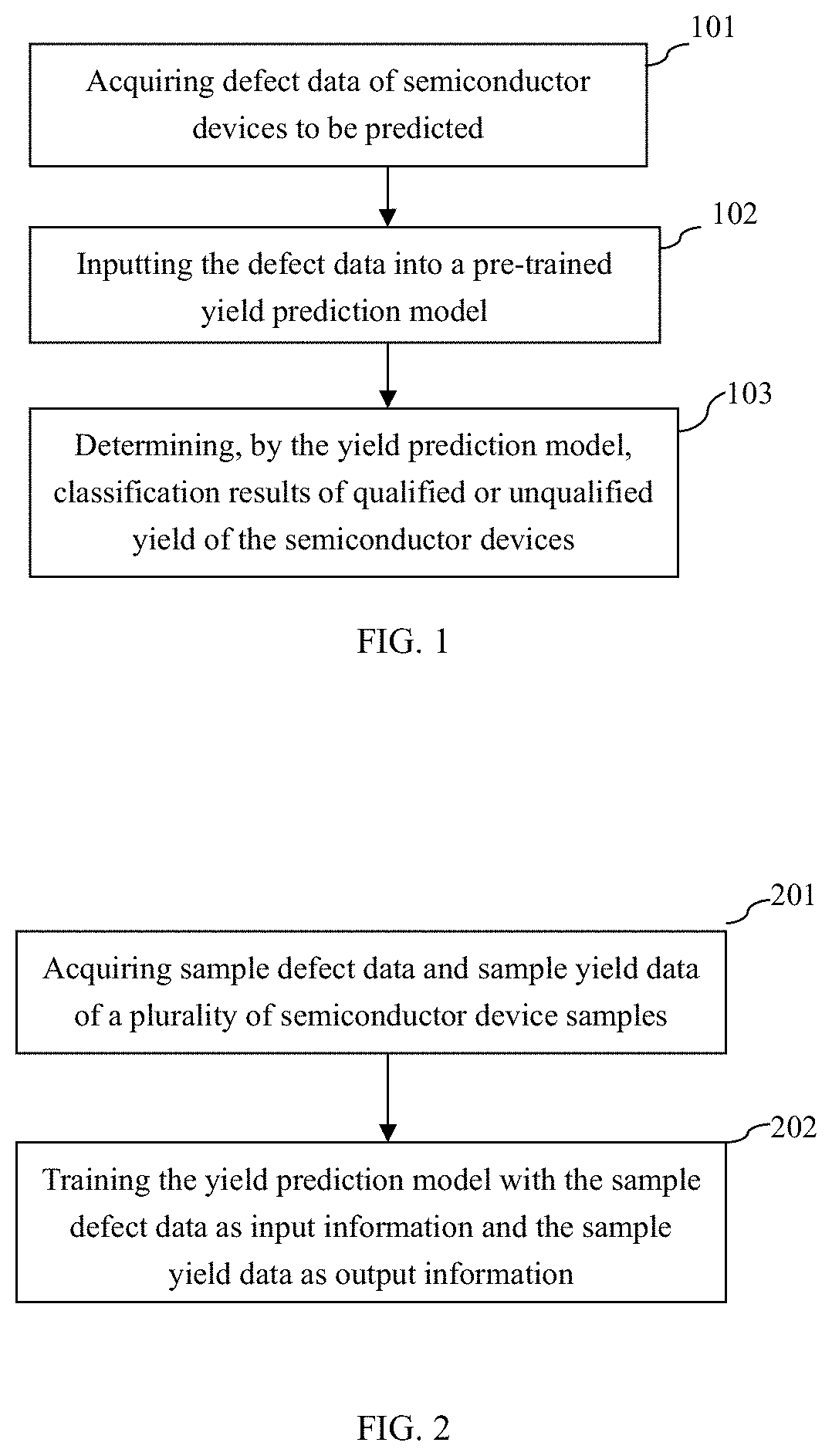
[0037]The following specific examples illustrate the embodiments of the present disclosure, and those skilled in the art can easily understand other advantages and effects of the present disclosure from the content disclosed in this specification. Although the description of the present disclosure will be introduced in conjunction with preferred embodiments, this does not mean that the features of the present disclosure are limited to the embodiments. On the contrary, the purpose of introducing the invention in conjunction with the embodiments is to cover other options or modifications that may be extended based on the claims of the present disclosure. In order to provide an in-depth understanding of the present disclosure, many specific details will be included in the following description. The present disclosure may also be implemented without using these details. In addition, in order to avoid confusion or obscuring the focus of the present disclosure, some specific details will ...


PUM


Abstract

A method for predicting the yield of manufacturing semiconductor devices includes steps of: acquiring defect data of semiconductor devices to be predicted, wherein the semiconductor devices to be predicted include finished semiconductor devices and semi-finished semiconductor devices, and the defect data indicates a defect type and location of at least one defect of the semiconductor devices; inputting the defect data into a pre-trained yield prediction model, wherein the yield prediction model includes a neural network structure and a classification structure, the neural network structure is used to extract defect feature vectors from the defect data, and the classification structure is used to output classification results of qualified or unqualified yield according to the defect feature vectors; and determining, by the yield prediction model, classification results of qualified or unqualified yield of the semiconductor devices.

Description

CROSS-REFERENCES TO RELATED APPLICATIONS[0001]This application claims the priority to Chinese patent application No. CN202011357825.0, filed on Nov. 27, 2020, and entitled “METHOD AND APPARATUS FOR PREDICTING YIELD OF SEMICONDUCTOR”, the disclosure of which is incorporated herein by reference in its entirety.TECHNICAL FIELD[0002]The present disclosure relates to a process managing technology for manufacturing semiconductor devices, in particular to a method for predicting the yield of manufacturing semiconductor devices and an apparatus for predicting the yield of manufacturing semiconductor devices.BACKGROUND[0003]With the increasing complexity of chip design, it is has become more difficult to put new chip designs into production. Chip manufacturers are looking for ways to speed up product launches and achieve the best yields they can. Mass data results show that production line defects directly affect the yields of chip products. Therefore, it is particularly important to monitor...

Claims


Application Information

Patent Timeline
Patent Type & Authority Applications(United States)
IPC IPC(8): G06N3/08
CPCG06N3/088G06N3/084G06N3/045G06F18/2411G06F18/214G06N20/10H01L22/20G06N3/044
Inventor CHEN, SHANSHANCHEN, HUNGLINLONG, YIN
Owner SHANGHAI HUALI INTEGRATED CIRCUIT CORP
Why Eureka
Try Eureka