Semiconductor package and method of manufacturing the semiconductor package

a semiconductor and semiconductor chip technology, applied in the direction of semiconductor devices, semiconductor/solid-state device details, electrical devices, etc., can solve the problems of bonding failure between the bonding pad of the semiconductor chip and the bonding pad of the wafer, and achieve the effect of improving the process yield of bonding a wafer and a di

Pending Publication Date: 2022-06-09
SAMSUNG ELECTRONICS CO LTD
View PDF19 Cites 7 Cited by
  • Summary
  • Abstract
  • Description
  • Claims
  • Application Information

AI Technical Summary

Benefits of technology

[0011]Accordingly, the second substrate recess and third substrate recess may prevent the metal residual materials from being formed between bonding surfaces of the second semiconductor chip and the third semiconductor chip and between the third semiconductor chip and the fourth semiconductor chip, to thereby prevent bonding failures due to the metal residual material. Thus, it may be possible to provide a stacked structure of a semiconductor package capable of improving a process yield of bonding a wafer and a die.

Problems solved by technology

As a result, a bonding failure between the bonding pad of the semiconductor chip and a bonding pad of the wafer may occur in a subsequent die-to-wafer hybrid bonding process.

Method used


Image

  • Semiconductor package and method of manufacturing the semiconductor package
  • Semiconductor package and method of manufacturing the semiconductor package
  • Semiconductor package and method of manufacturing the semiconductor package

Examples


Embodiment Construction

[0020]Hereinafter, example embodiments will be explained in detail with reference to the accompanying drawings.

[0021]It will be understood that, although the terms first, second, third etc. may be used herein to describe various elements or components, these elements or components should not be limited by these terms. These terms are only used to distinguish one or more elements or components from another one or more elements or components. Thus, for example, a first bonding pad discussed below could be termed a third bonding pad or a fourth bonding pad, a second recess discussed below could be termed a first recess, and so on, without departing from the teachings of the inventive concept(s) described herein.

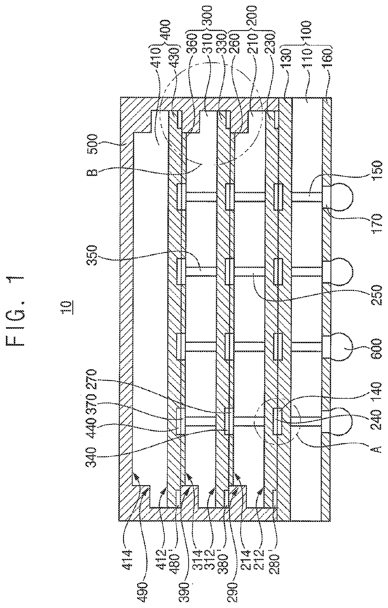
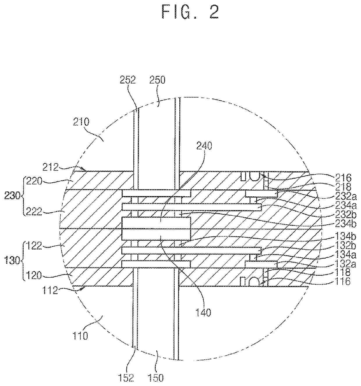
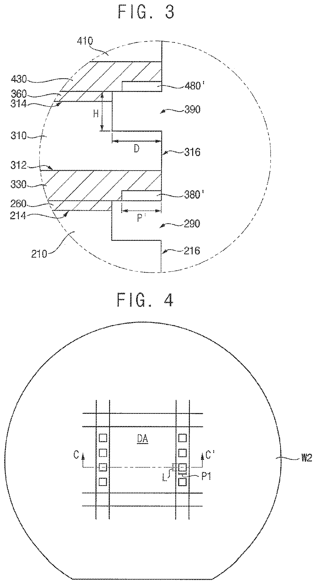
[0022]FIG. 1 is a cross-sectional view illustrating a semiconductor package in accordance with example embodiments. FIG. 2 is an enlarged cross-sectional view illustrating portion ‘A’ in FIG. 1. FIG. 3 is an enlarged cross-sectional view illustrating portion ‘B’ in FIG. 1.

[0023]...


PUM

PropertyMeasurementUnit
widthaaaaaaaaaa
widthaaaaaaaaaa
widthaaaaaaaaaa

Abstract

A semiconductor package includes a first semiconductor chip, a second semiconductor chip, a third semiconductor chip and a fourth semiconductor chip sequentially stacked on one another. The second semiconductor chip includes a second substrate and a second substrate recess formed in an edge of a backside surface of the second substrate. The third semiconductor chip includes a third substrate and a first metal residual material provided in a peripheral region of a front surface of the third substrate. When the second semiconductor chip and the third semiconductor chip are bonded to each other such that the front surface of the third substrate and the backside surface of the second substrate face each other, the first metal residual material is located in the second substrate recess. A first bonding pad on the backside surface of the second substrate and a second bonding pad on the front surface of the third substrate are bonded to each other.

Description

CROSS-REFERENCE TO RELATED APPLICATION[0001]This U.S. nonprovisional patent application claims priority under 35 U.S.C. § 119 to Korean Patent Application No. 10-2020-0170458, filed on Dec. 8, 2020 in the Korean Intellectual Property Office (KIPO), the contents of which are herein incorporated by reference in their entirety.BACKGROUND1. Field[0002]Example embodiments relate to a semiconductor package and a method of manufacturing the semiconductor package. More particularly, example embodiments relate to a semiconductor package including semiconductor chips stacked by a die-to-wafer bonding process and a method of manufacturing the same.2. Description of the Related Art[0003]In order to manufacture a multi-chip package in which at least two semiconductor chips are stacked, in a die-to-wafer bonding process, pad-to-pad direct bonding may be performed without using solder bumps.[0004]However, in order to dice a wafer, a sawing process may be performed on a front surface of the wafer a...

Claims


Application Information

Patent Timeline
Patent Type & Authority Applications(United States)
IPC IPC(8): H01L25/065H01L29/06H01L23/00
CPCH01L25/0657H01L2224/08146H01L24/08H01L29/0684H01L29/0657H01L21/76898H01L2224/32145H01L2924/181H01L2924/10158H01L2224/08145H01L2224/94H01L21/78H01L2225/06555H01L2225/06541H01L2225/06586H01L23/3128H01L21/561H01L21/568H01L23/3135H01L21/6835H01L2221/68327H01L2221/68345H01L2221/68354H01L2924/00012H01L2224/80H01L23/13H01L23/485H01L23/544H01L24/06H01L24/09H01L23/49827
Inventor KIM, JUNGHWANPARK, SANGCHEON
Owner SAMSUNG ELECTRONICS CO LTD
Why Eureka
Try Eureka