Inspection Apparatus Adjustment System and Inspection Apparatus Adjustment Method

Pending Publication Date: 2022-08-11
HITACHI HIGH-TECH CORP
View PDF0 Cites 0 Cited by
  • Summary
  • Abstract
  • Description
  • Claims
  • Application Information

AI Technical Summary

Benefits of technology

[0012]According to the present invention, the

Problems solved by technology

Since an adjustment work is a complicated work of handling a plurality of optical conditions, it is difficult to perform the adjustment work unless a person understands the mechan

Method used


Image

  • Inspection Apparatus Adjustment System and Inspection Apparatus Adjustment Method
  • Inspection Apparatus Adjustment System and Inspection Apparatus Adjustment Method
  • Inspection Apparatus Adjustment System and Inspection Apparatus Adjustment Method

Examples


first embodiment

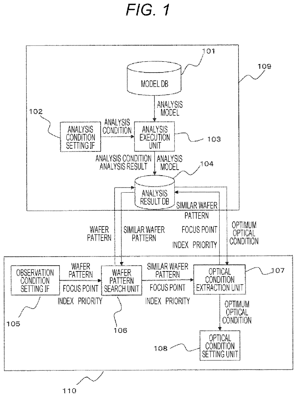
[0025]FIG. 1 illustrates an inspection apparatus automatic adjustment system according to a first embodiment. The inspection apparatus automatic adjustment system includes a model DB 101, an analysis condition setting IF 102, an analysis execution unit 103, an analysis result DB 104, an observation condition setting IF 105, a wafer pattern search unit 106, an optical condition extraction unit 107, and an optical condition setting unit 108. The model DB 101, the analysis condition setting IF 102, the analysis execution unit 103, and the analysis result DB 104 are defined as an analysis result DB creation unit 109, and the observation condition setting IF 105, the wafer pattern search unit 106, the optical condition extraction unit 107, and the optical condition setting unit 108 are defined as an optimum optical condition extraction unit 110.

[0026]A configuration of the analysis result DB creation unit 109 will be described. In the analysis result DB creation unit 109, analysis condit...

second embodiment

[0049]Next, FIG. 9 illustrates an inspection apparatus automatic adjustment system according to a second embodiment. In the second embodiment, the analysis result DB creation unit 109 is connected to various apparatuses and databases via a network 901. The specification can be received via the network 901, and the analysis result DB 104 can be shared by a plurality of inspection apparatuses. That is, a cloud configuration of the analysis result DB creation unit 109 is realized.

[0050]For example, when the specification of the wafer to be inspected is greatly different even after the delivery of the inspection apparatus, it is necessary to set the optical condition again, but it is assumed that there is no model of the wafer in the model DB. Thus, the analysis result DB creation unit 109 of the inspection apparatus automatic adjustment system is constructed in a PC in the inspection apparatus manufacturer, and the optimum optical condition extraction unit 110 is provided in the inspec...

third embodiment

[0052]FIG. 10 illustrates another example of the method of extracting the optimum optical condition illustrated in FIG. 8. This is an extraction flow of the optimum optical condition on the assumption that a width of a deep hole bottom is measured. In order to measure the width with high accuracy, it is necessary to focus on the bottom, but a depth may vary in an actual wafer. Processing performed by the optical condition extraction unit 107 for solving this problem will be described below.

[0053]First, an estimated value of the variation in depth is set (step 1001). This is set based on past actual values and information from the customer. For example, a deviation in depth included in a depth actual value in the past inspection input via the observation condition setting IF 105 or information from the customer is calculated and used as an estimated value.

[0054]Subsequently, the optimum optical condition obtained from the analysis model (wafer model and inspection apparatus model) in...


PUM


Abstract

The present invention addresses the problem of quickly specifying an optical condition of a wafer to be inspected, and in particular, accelerating optical condition setting after obtaining a customer wafer. An inspection apparatus automatic adjustment system according to the present invention comprises: an analysis condition setting interface 102 which inputs analysis conditions; an analysis execution unit 103 which performs analysis; an inspection device model and model DB 101 used for analysis; an analysis result DB 104 that stores analysis results; an observation condition setting interface 105 which inputs a wafer pattern, a focus point, an optimization index, and a priority; a wafer pattern search unit 106 which searches for a wafer pattern similar to the input wafer pattern; an optical condition extraction unit 107 which extracts, from the analysis result DB 104, the optimum optical condition for the similar wafer pattern and the focus point; and an optical condition setting unit 108 which generates a control signal corresponding to the optical condition and transmits the control signal to the inspection apparatus.

Description

TECHNICAL FIELD[0001]The present invention relates to a technology for automatically adjusting an inspection apparatus of a sample. The sample includes a semiconductor wafer (hereinafter, also referred to as a wafer). The inspection apparatus also includes an observation apparatus.BACKGROUND ART[0002]As an inspection apparatus that obtains an image by irradiating a sample with an electron beam (primary electrons) and detecting signal electrons (secondary electrons) secondarily generated from the sample, there is a scanning electron microscope (SEM). An inspection apparatus that inspects a semiconductor wafer includes inspection apparatuses using the SEM, and one of the inspection apparatuses is a critical dimension SEM (CD-SEM). Semiconductors are becoming finer year by year, and there is an increasing demand for improvement of resolution and measurement reproducibility, reduction of measurement errors between the inspection apparatuses, and the like for the CD-SEM. In order to obta...

Claims


Application Information

Patent Timeline
IPC IPC(8): G01N21/95G01N23/2251G06T7/00
CPCG01N21/9501G01N23/2251G06T2207/30148G01N2223/6116G06T2207/10061G06T7/0004G03F7/70625G03F7/705H01J2237/2816H01J37/265H01J2237/216H01J37/28H01L22/12G01N2223/646
Inventor MAEDA, TAICHISASAKI, YUKO
Owner HITACHI HIGH-TECH CORP
Why Eureka
Try Eureka