Test socket assembly

a technology of socket assembly and test socket, which is applied in the direction of electronic circuit testing, measurement devices, instruments, etc., can solve the problems of increasing the difficulty of installing the device guide on the tester board, not easy to manufacture a suitable device guide, and the difficulty of using the pogo pin type test socket in the test requiring a communication speed of 1 ghz, etc., to achieve stable transmission of signals, reduce manufacturing costs, and simple structure

Pending Publication Date: 2022-08-11
SHIN JONG CHOEN +1
View PDF5 Cites 2 Cited by
  • Summary
  • Abstract
  • Description
  • Claims
  • Application Information

AI Technical Summary

Benefits of technology

[0021]In the test socket assembly according to the present disclosure, since the test socket having the electro-conductive part for transmitting the signal is mounted to the socket supporting part protruding from the housing body of the guide housing to which the tester board is installed, the test socket may come into smooth contact with the board terminal without interfering with the passive element installed on the tester board. Therefore, it is possible to stably transmit the signal to the test socket having a single-layered structure without utilizing the conventional test socket having a multi-layered structure in which a plurality of elements is stacked. In addition, by employing the test socket having a single-layered structure, this test socket may be utilized for a test requiring a high-speed communication speed.
[0022]In addition, in the test socket assembly according to the present disclosure, the test socket may be simply coupled to the guide housing through the socket frame having a bent structure. Therefore, the structure is simple, the manufacturing cost may be reduced, and the manufacturing time may be shortened.

Problems solved by technology

However, as the number of passive elements installed on the tester board is increased, it is becoming increasingly difficult to install the device guide on the tester board.
Therefore, in the case of a pogo pin type test socket, it is not difficult to manufacture a device guide suitable for the pogo pin.
Therefore, it is difficult to utilize the pogo pin type test socket in the test requiring a communication speed of 1 GHz or higher.
However, the conventional anisotropic electro-conductive socket has a disadvantage in that it is impossible to manufacture it having a height of 1 mm or more.
In addition, since the conventional test socket 1 has a stacked structure consisting of a plurality of elements, it has drawbacks in that since there are many contact points between elements, electrical resistance is increased, and manufacturing cost is increased.

Method used


Image

  • Test socket assembly
  • Test socket assembly
  • Test socket assembly

Examples


Embodiment Construction

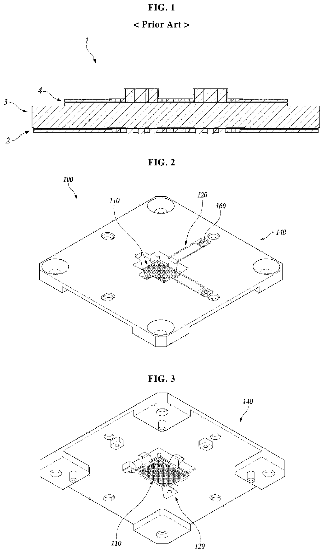
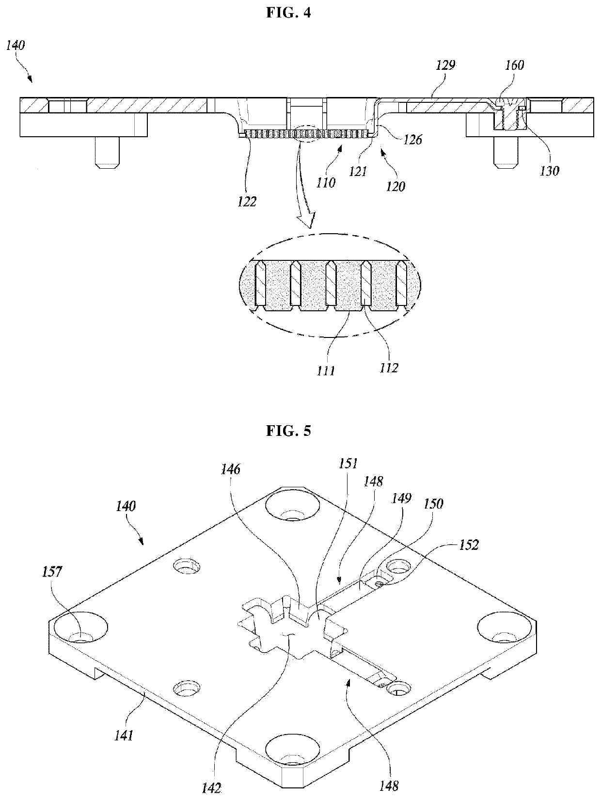
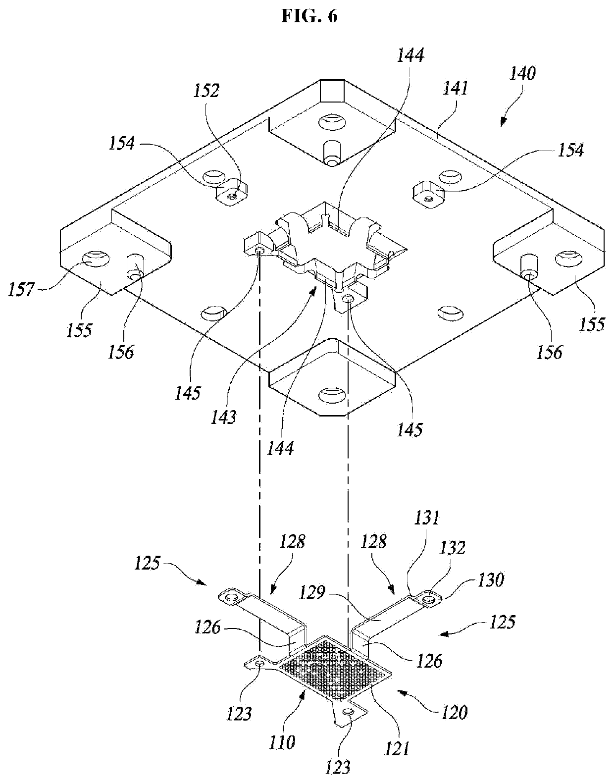
[0033]Hereinafter, a test socket assembly according to the present disclosure is described in detail with reference to the drawings.

[0034]FIGS. 2 and 3 are perspective views showing a test socket assembly according to one embodiment of the present disclosure, FIG. 4 is a cross-sectional view showing the test socket assembly according to one embodiment of the present disclosure, FIG. 5 is a perspective view showing a guide housing of the test socket assembly according to one embodiment of the present disclosure, FIGS. 6 and 7 are views for explaining an assembling process of the test socket assembly according to one embodiment of the present disclosure, and FIG. 8 is a view showing a use case in which the test socket assembly according to one embodiment of the present disclosure is used.

[0035]As illustrated in the drawings, a test socket assembly 100 according to one embodiment of the present disclosure is provided for transmitting an electrical signal between a device 20 under test ...


PUM


Abstract

A test socket assembly which can stably transmit a signal at high communication speed comprises: a test socket having a plurality of conductive parts for electrically connecting a device terminal of the device to be tested and a board terminal of the tester board; a guide housing including a housing body having a housing opening into which the device to be tested can be inserted, and a socket supporting section disposed beneath the housing opening so as to protrude from one surface of the housing body; and a socket frame including a frame body, which is coupled to the test socket so as to be secured to the socket supporting section so that the test socket is supported beneath the housing opening, and a frame wing which is bent from the frame body toward the housing body so as to be secured to the housing body.

Description

TECHNICAL FIELD[0001]The present disclosure relates to a test socket assembly, and more particularly, to a test socket assembly capable of transmitting an electrical signal between a device under test and a tester board.BACKGROUND ART[0002]After a process for manufacturing a semiconductor device is completed, it is necessary to test the semiconductor device. When performing a test for the semiconductor device, a test socket configured to electrically connect a test equipment and the semiconductor device is required. In the test process, the test socket is an intermediary component by which a signal generated from a tester can be transmitted to the semiconductor device.[0003]In order to perform a reliable test of the semiconductor device, it is necessary to accurately align a terminal of the semiconductor device and the test socket to each other. When testing the semiconductor device, a device guide is employed so as to accurately position the semiconductor device. The device guide i...

Claims


Application Information

Patent Timeline
Patent Type & Authority Applications(United States)
IPC IPC(8): G01R1/04H01R13/73G01R31/28
CPCG01R1/0416G01R31/2851H01R13/73H01R12/00G01R1/045G01R1/07357G01R1/0466G01R1/0735G01R31/2886
Inventor SHIN, JONG CHOENHA, DONG HO
Owner SHIN JONG CHOEN
Why Eureka
Try Eureka