
INTEGRATED CIRCUITS (ICs) WITH MULTI-ROW COLUMNAR DIE INTERCONNECTS AND IC PACKAGES INCLUDING HIGH DENSITY DIE-TO-DIE (D2D) INTERCONNECTS

a technology of integrated circuits and columnar dies, which is applied in the field of integrated circuits with multi-row columnar die interconnects and ic packages including high density die-to-die (d2d) interconnects, can solve the problems of increasing product cost, reducing manufacturing yield, and limited number of die-to-die connections that can be placed at the opposing edges, so as to reduce the length of d2d interconnects

Active Publication Date: 2022-09-08
QUALCOMM INC
View PDF3 Cites 0 Cited by
  • Summary
  • Abstract
  • Description
  • Claims
  • Application Information

AI Technical Summary

Benefits of technology

The patent text describes an integrated circuit (IC) package with multi-row columnar die interconnects and high density die-to-die (D2D) interconnects. By closely integrating ICs in the package and positioning them edge to edge, the D2D interconnects are minimized and the number of interconnects is maximized. By using die interconnect columns with a greater distance between columns, additional interconnects can be used at the D2D interconnect pitch between columns. This results in a more dense arrangement of ICs in the package. Overall, the patent text provides a solution for enhancing IC integration in an integrated circuit package.

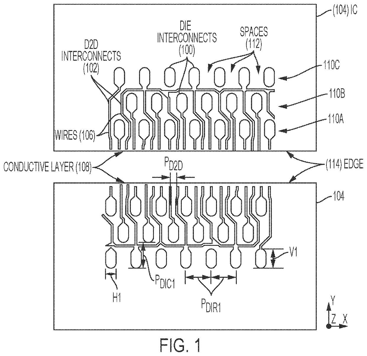
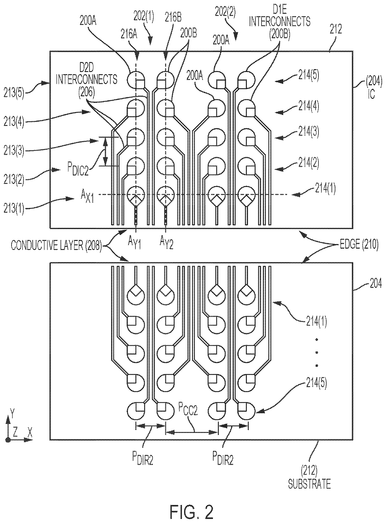
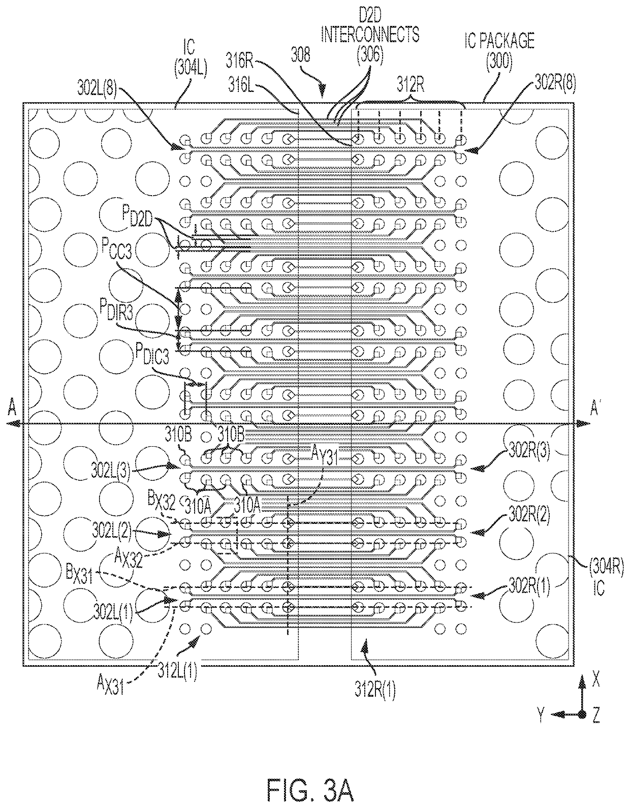
Problems solved by technology

As an IC increases in area and complexity, manufacturing yields are diminished, which increases product cost.
However, for two separate IC dies to approach the level of performance of a single IC requires a close level of integration, which may require high bandwidth interconnectivity between the IC dies.
The number of die to die connections that can be placed at the opposing edges is limited by dimensions of the interconnect structures and technology requirements.

Method used


Image

  • INTEGRATED CIRCUITS (ICs) WITH MULTI-ROW COLUMNAR DIE INTERCONNECTS AND IC PACKAGES INCLUDING HIGH DENSITY DIE-TO-DIE (D2D) INTERCONNECTS
  • INTEGRATED CIRCUITS (ICs) WITH MULTI-ROW COLUMNAR DIE INTERCONNECTS AND IC PACKAGES INCLUDING HIGH DENSITY DIE-TO-DIE (D2D) INTERCONNECTS
  • INTEGRATED CIRCUITS (ICs) WITH MULTI-ROW COLUMNAR DIE INTERCONNECTS AND IC PACKAGES INCLUDING HIGH DENSITY DIE-TO-DIE (D2D) INTERCONNECTS

Examples


Embodiment Construction

[0013]With reference now to the drawing figures, several exemplary aspects of the present disclosure are described. The word “exemplary” is used herein to mean “serving as an example, instance, or illustration.” Any aspect described herein as “exemplary” is not necessarily to be construed as preferred or advantageous over other aspects.

[0014]Aspects disclosed herein include integrated circuits (ICs) with multi-row columnar die interconnects and IC packages including high density die-to-die (D2D) interconnects. Closely integrated ICs in an IC package are positioned edge to edge to minimize the length of D2D interconnects disposed along the IC edges. A maximum number of D2D interconnects in a conductive layer that fit along the length of the IC edge depends on the center-to-center distance or pitch of the D2D interconnects and also on the pitch of the die interconnects (e.g., bumps or studs) to which the D2D interconnects are coupled. The die interconnect pitch, which is significantly...


PUM


Abstract

An integrated circuit (IC) package including ICs with multi-row columnar die interconnects has increased die-to-die (D2D) interconnect density in a conductive layer. Positioning the die interconnects in die interconnect column clusters, that each include a plurality of die interconnect rows and two columns, reduces the linear dimension occupied by the die interconnects and leaves room for more D2D interconnects. A die interconnect column cluster pitch is a distance between columns of adjacent die interconnect column clusters and this distance is greater than a die interconnect pitch between columns within the column clusters. Die interconnects may be disposed in the space between the multi-row column clusters and additional die interconnects can be disposed at the D2D interconnect pitch between the die interconnect column clusters. IC packages with ICs including the multi-row columnar die interconnects have a greater number of D2D interconnects for better IC integration.

Description

BACKGROUNDI. Field of the Disclosure[0001]The field of the disclosure relates generally to integrated circuits (ICs) and more specifically to interconnecting dies in IC packages.II. Background[0002]Manufacturers of consumer electronic devices seek to maximize device performance while minimizing device size because users prefer smaller devices and they are cheaper to manufacture. The functionality and performance of electronic devices is provided by integrated circuits (ICs). One way to increase the performance of an IC is to add circuitry which increases the size and complexity of the IC. As an IC increases in area and complexity, manufacturing yields are diminished, which increases product cost. An alternative approach to maximizing performance of an electronic device is to split the functionality among two or more IC dies in an IC package. Reducing the size and complexity of the IC dies improves yield. However, for two separate IC dies to approach the level of performance of a sin...

Claims


Application Information

Patent Timeline
Patent Type & Authority Applications(United States)
IPC IPC(8): H01L23/538H01L23/00H01L25/065
CPCH01L23/5386H01L24/16H01L24/17H01L25/0655H01L2224/16157H01L2224/1712H01L2924/37001H01L2224/24137H01L2924/18162H01L2224/16227H01L2924/15192H01L24/20H01L2224/0401H01L2224/131H01L2224/13147H01L2224/13124H01L2224/214H01L2224/96H01L24/13H01L2224/06152H01L2224/06156H01L2224/14152H01L2224/14156H01L24/06H01L24/14H01L2924/014H01L2924/00014
Inventor ZHOU, RONGADERHOLDT, WILLIAM M.
Owner QUALCOMM INC
Learn More