An athermal arrayed waveguide grating

a waveguide grating and array technology, applied in the direction of optical waveguide light guides, instruments, optics, etc., can solve the problems of complex structural design and process methods, limited use of active temperature control in the working environment, etc., and achieve the effect of simplifying the structure of the athermal arrayed waveguide grating

Active Publication Date: 2022-09-15
SUZHOU YIRUI OPTOELECTRONICS TECH CO LTD
View PDF4 Cites 0 Cited by
  • Summary
  • Abstract
  • Description
  • Claims
  • Application Information

AI Technical Summary

Benefits of technology

[0017]the waveguide core layer comprises multilayer structures having a periodic configuration, the multilayer structure comprises two layers of silica material and a negative temperature coefficient material disposed between the two layers of silica material; the negative temperature coefficient material is used to compensate for a dimensional deformation of the silicon-based substrate after being heated, so as to reduce the temperature drift coefficient of the athermal arrayed waveguide grating.
[0024]The beneficial effect of the present invention is: the technical scheme of the present invention overcomes a problem that the structure of the athermal arrayed waveguide grating is difficult to design, eliminates the additional structures and assembly processes, and simplifies the structure of the athermal arrayed waveguide grating. And by setting the negative temperature coefficient material in the waveguide core layer structure, the present invention makes the grating athermal, thus ensuring that the temperature drift coefficient of the grating satisfies requirements, and athermal operation conditions are met.

Problems solved by technology

In order to keep the central wavelength of the AWG unchanged at different ambient temperatures and reduce the temperature drift coefficient of its central wavelength, the traditional technology is to use a temperature control device, such as heater or electric refrigerating unit to stable the working temperature of the AWG, which need to provide additional power input, and the use of active temperature control is limited in the working environment with large temperature difference.
The conventional athermal technology requires additional mechanical structure to the grating to compensate the wavelength-temperature drift, which requires more complex structural design and process methods.

Method used


Image

  • An athermal arrayed waveguide grating

Examples


embodiment 1

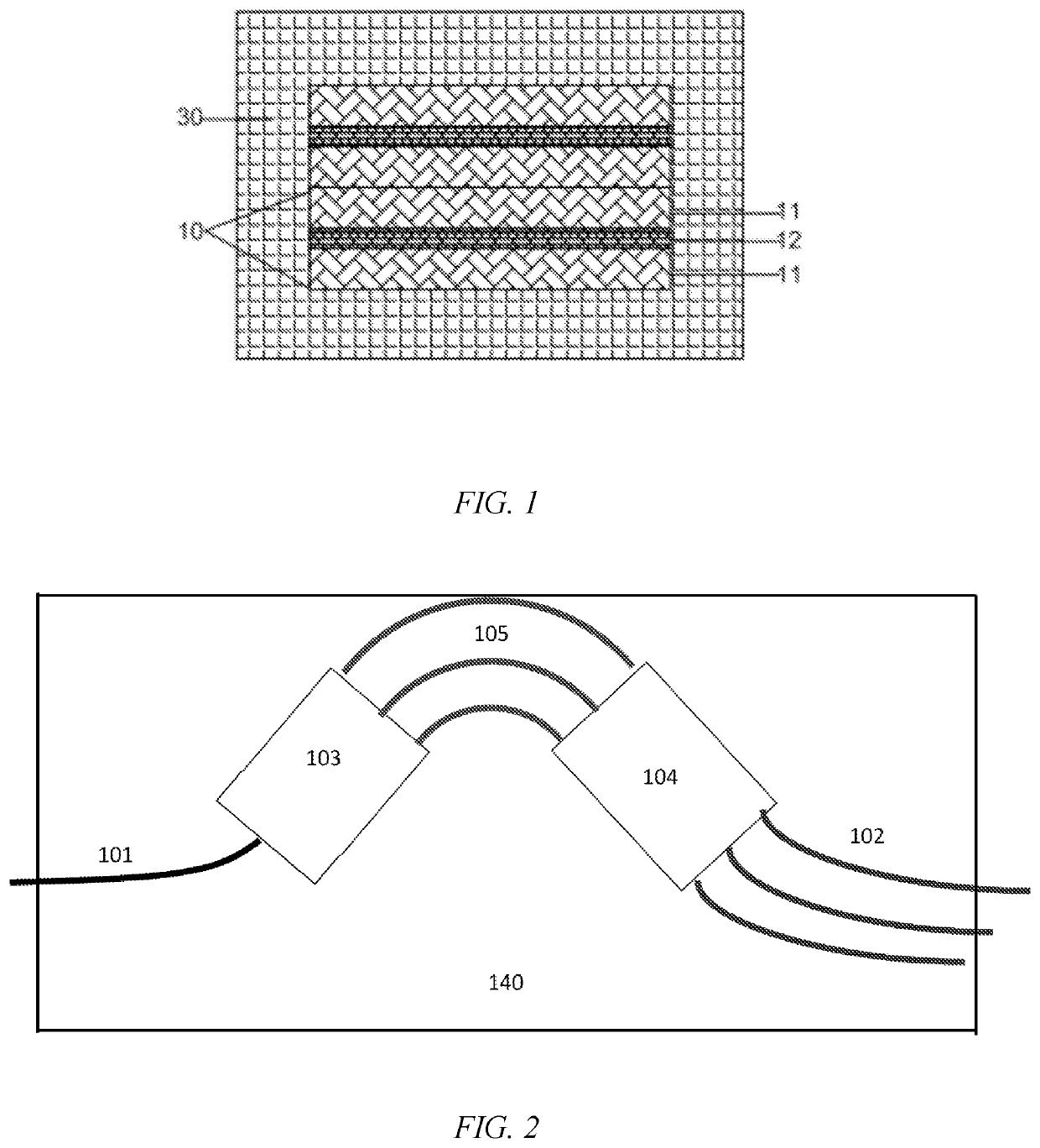
[0029]Referring to FIG. 1, which shows an athermal arrayed waveguide, including a silica cladding layer (30) and a waveguide core layer disposed in the cladding layer (30), the waveguide core layer comprises multilayer structure (10), which comprises two layers of silica material (11) and negative temperature coefficient material (12) disposed between the two layers of silica material; the negative temperature coefficient material (12) is used to compensate for a dimensional deformation of the silicon-based substrate (140) after being heated, so as to reduce the temperature drift coefficient of the athermal arrayed waveguide grating.

[0030]In this embodiment, the refractive index of the waveguide core layer is greater than that of the silica cladding layer (30).

[0031]In the embodiment, the negative temperature coefficient material (12) is titanium dioxide.

[0032]In the embodiment, in the multilayer structure (10), the thickness of the silica material (11) is 0.5-1 μm, and the thicknes...

embodiment 2

[0036]Referring to FIG. 2, the present invention also shows an athermal arrayed waveguide grating device, which includes a silicon-based substrate (140), and the following structure disposed on the silicon-based substrate (140):[0037]one input waveguide (101) for inputting optical signal;[0038]a first free transmission region (103), composed of a first planar waveguide and coupled with the output end of the input waveguide (101);[0039]the athermal arrayed waveguide (105) shown in the embodiment 1, coupled with the output end of the first free transmission region (103);[0040]a second free transmission region (104), composed of a second planar waveguide and coupled with the output end of the athermal arrayed waveguide (105);[0041]and at least one output waveguide (102) for outputting optical signal, coupled with the output end of the second free transmission region (104).

[0042]The temperature drift coefficient of the central wavelength of the grating device with the waveguide structur...


PUM

PropertyMeasurementUnit
thicknessaaaaaaaaaa
thicknessaaaaaaaaaa
refractive indexaaaaaaaaaa

Abstract

An athermal arrayed waveguide grating includes a silicon-based substrate and an athermal arrayed waveguide disposed on the silicon-based substrate. The athermal arrayed waveguide includes a cladding layer and a waveguide chip layer, the waveguide chip layer is disposed on the cladding layer and has a refractive index greater than that of the cladding layer; the waveguide core layer includes multilayer structures having a periodic configuration, the multilayer structure includes two layers of silica material and a negative temperature coefficient material disposed between the two layers of silica material; the negative temperature coefficient material is used to compensate for a dimensional deformation of the silicon-based substrate after being heated. The present invention simplifies the structure of the athermal arrayed waveguide grating, sets the negative temperature coefficient material in the waveguide core layer structure, and makes the final temperature coefficient of refractive index of the waveguide structure is a negative number.

Description

CROSS REFERENCE TO RELATED APPLICATIONS[0001]This application claims priority of Chinese Patent Application No. 201910812393.9, filed Aug. 30, 2019, the entire disclosures of both of which are incorporated herein by reference.FIELD OF THE INVENTION[0002]The present invention relates to the planar optical waveguide devices, and belongs to an anthermal arrayed waveguide grating.DESCRIPTION OF THE PRIOR ART[0003]AWG (Arrayed Waveguide Grating) is a kind of angular-dispersion passive device, which based on planar optical waveguide technology and was first proposed by Smit in the late 1980s, and then it has attracted the attention of Bell Research Institute, NTT and other research institutions. With the development of planar optical waveguide technology, the corresponding products are gradually commercialized. Compared with other WDM (Wavelength Division Multiplexing) devices, AWG has the advantages of flexible design, low insertion loss, good filtering performance, long-term stability a...

Claims


Application Information

Patent Timeline
Patent Type & Authority Applications(United States)
IPC IPC(8): G02B6/12G02B6/122
CPCG02B6/12011G02B6/12016G02B6/1223G02B6/12009G02B6/12026G02B6/12028
Inventor CHEN, YIFANZHENG, RUI
Owner SUZHOU YIRUI OPTOELECTRONICS TECH CO LTD
Why Eureka
Try Eureka