

A Full CMOS Reference Voltage Source with High Power Supply Rejection Ratio
A technology with high power supply rejection ratio and reference voltage source, applied in the direction of regulating electrical variables, control/regulation systems, instruments, etc., can solve the problems of low power supply rejection, large reference voltage source layout area, high power consumption, and achieve low power supply voltage Adjustment rate, low power consumption, the effect of reducing production cost
- Summary
- Abstract
- Description
- Claims
- Application Information
AI Technical Summary
Problems solved by technology
Method used
Image

Examples
Embodiment Construction
[0016] Below in conjunction with accompanying drawing and embodiment, describe technical solution of the present invention in detail:
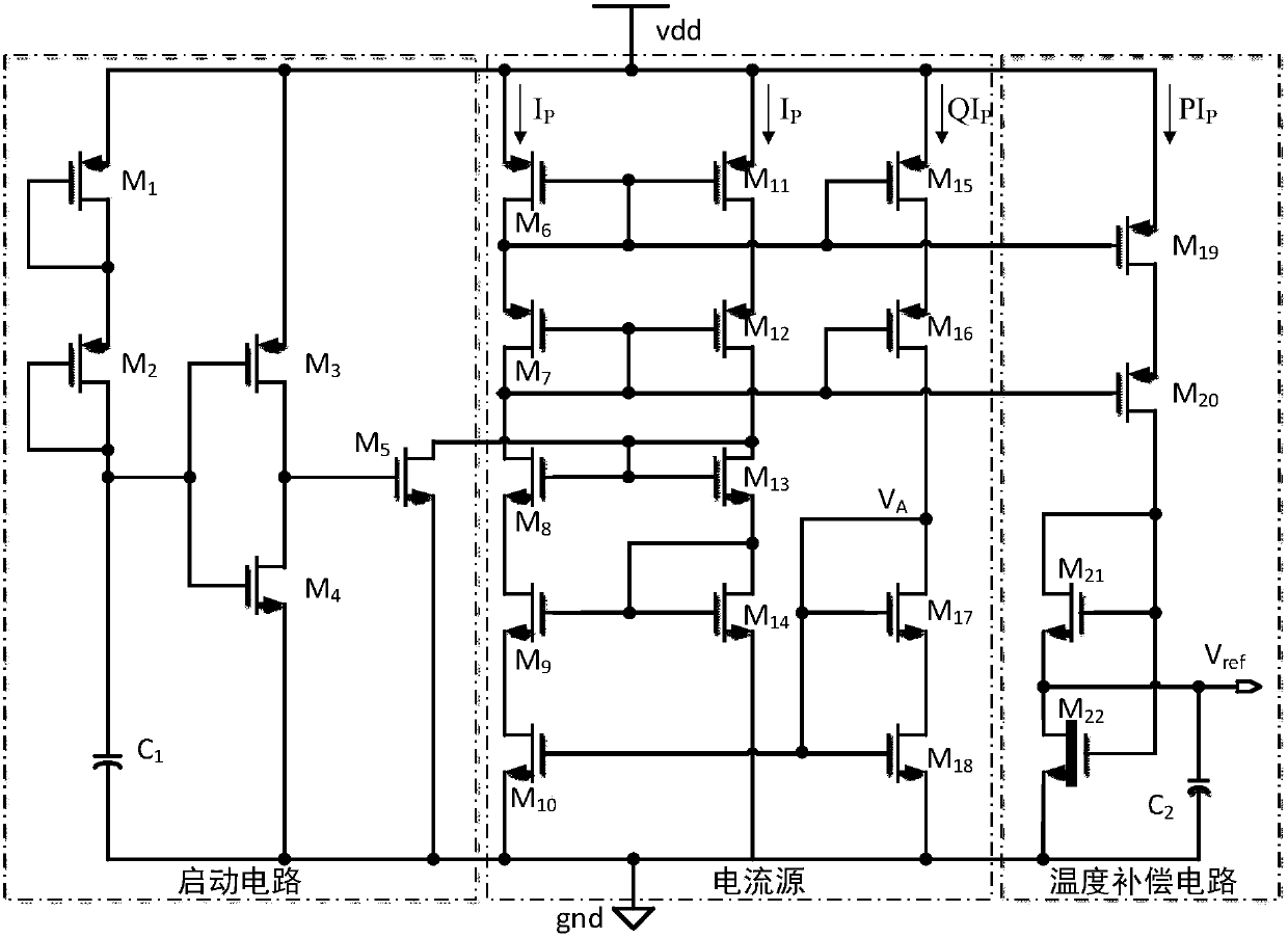
[0017] A high power supply rejection ratio full CMOS voltage reference, such as figure 1 Shown, including start-up circuit, current source and temperature compensation circuit. The output terminal of the start-up circuit is connected to the input terminal of the current source circuit, the output terminal of the current source circuit is connected to the input terminal of the temperature compensation circuit, and the output terminal of the temperature compensation circuit forms the output terminal V of the entire reference voltage source. ref .
[0018] The start-up circuit provides current when the reference voltage source is turned on, so that the reference voltage source gets rid of the degenerate bias point and enters a normal working state. In a preferred embodiment of the present invention, the above startup circuit includes a PMOS tra...
PUM
 Abstract
Description
Claims
Application Information