Integrated optical sensor and method of manufacturing the same

a technology of integrated optical sensor and manufacturing method, which is applied in the direction of instruments, lenses, radio frequency control devices, etc., can solve the problems of poor precision of optical sensor, high cost, and complex manufacturing process of overall optical sensor

Pending Publication Date: 2022-09-15
EGIS TECH
View PDF0 Cites 6 Cited by
  • Summary
  • Abstract
  • Description
  • Claims
  • Application Information

AI Technical Summary

Problems solved by technology

The prior art optical sensor has a filter layer and a lens, which are formed by a package process and cannot be integrated in a semiconductor process of forming a sensing chip including sensing pixels.
Thus, the optical sensor cannot be manufactured in an integrated manner.
Therefore, the manufacturing process of the overall optical sensor is complicated, and the optical sensor has the poor precision and the high cost.

Method used


Image

  • Integrated optical sensor and method of manufacturing the same
  • Integrated optical sensor and method of manufacturing the same
  • Integrated optical sensor and method of manufacturing the same

Examples


Embodiment Construction

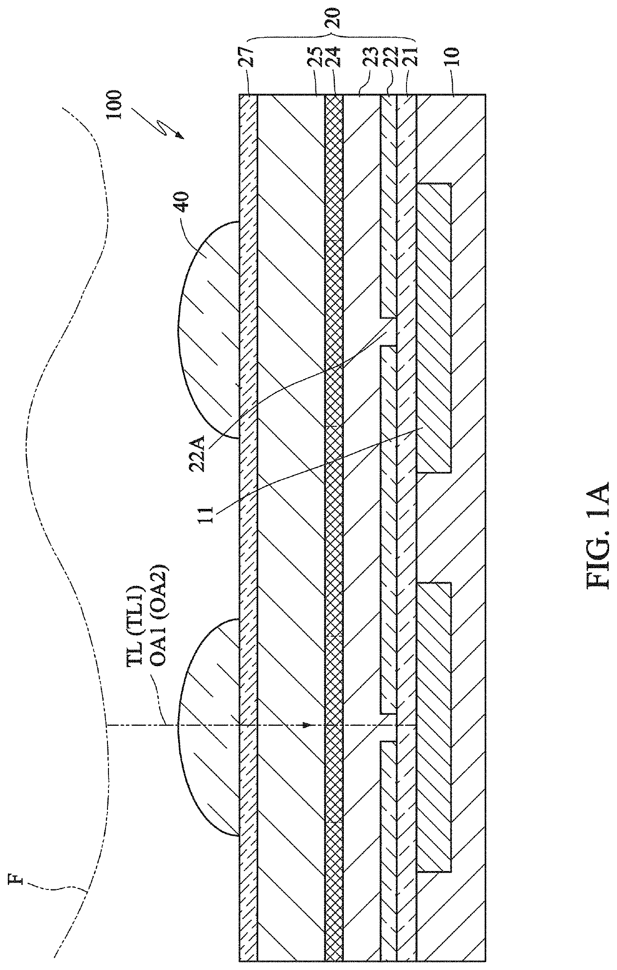
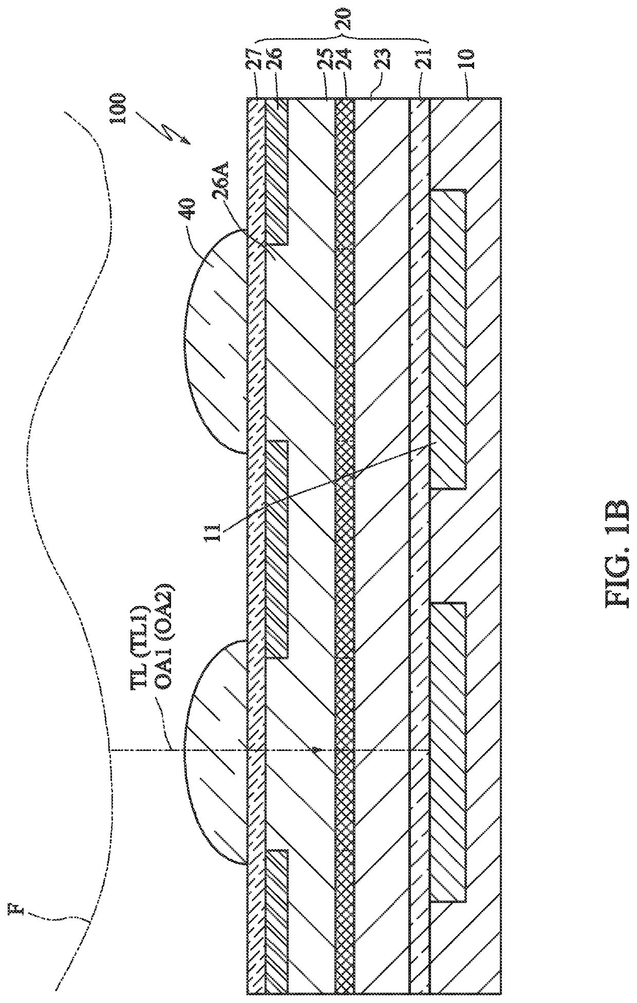
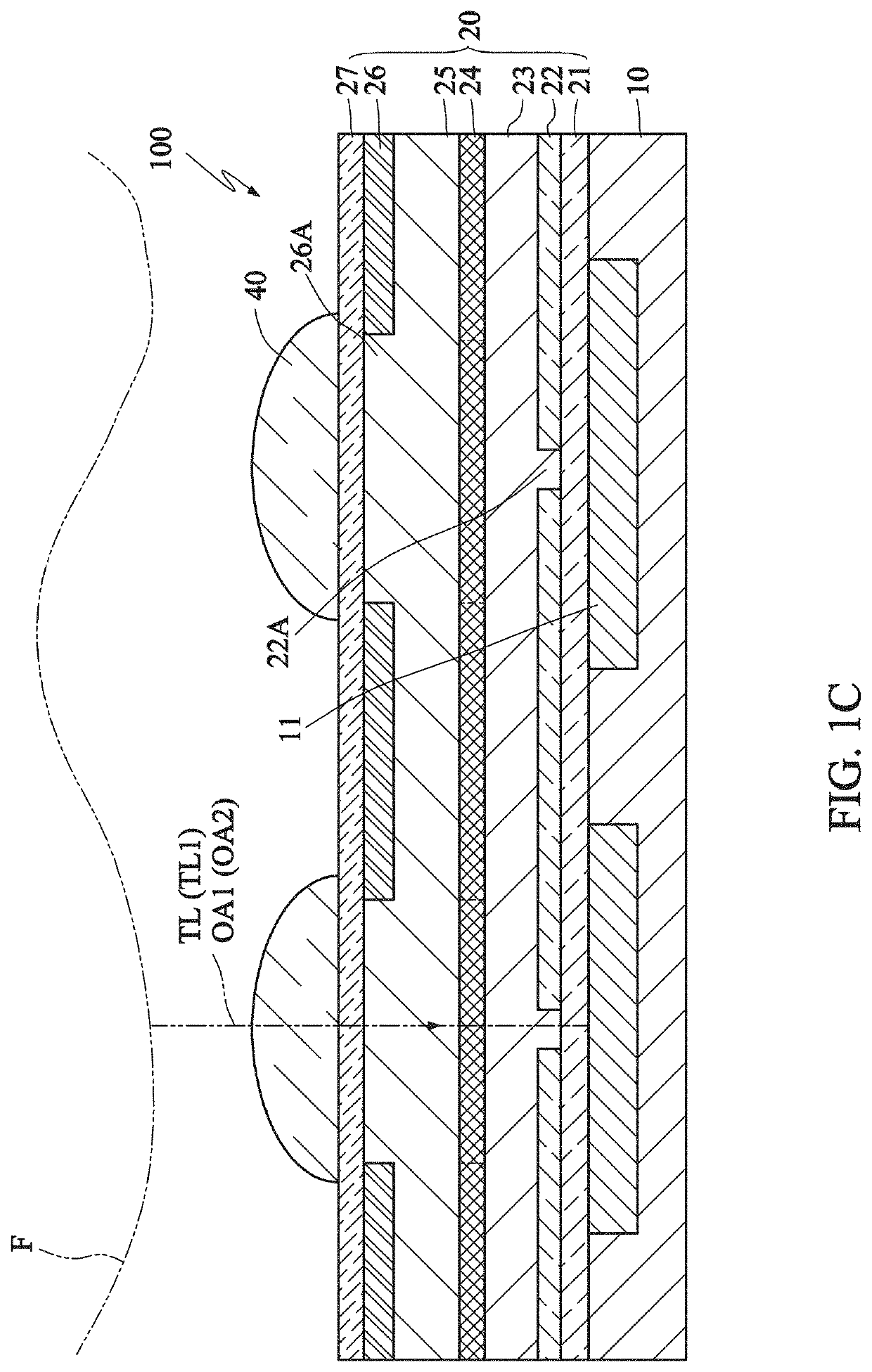
[0058]FIGS. 1A to 1C are schematically partial cross-sectional views showing several examples of an integrated optical sensor 100 according to a preferred embodiment of this disclosure. Referring to FIG. 1A, the integrated optical sensor 100 includes a substrate 10 (e.g., a semiconductor substrate, such as a silicon substrate), an optical module layer 20 and multiple micro lenses 40. The substrate 10 has multiple sensing pixels 11. The optical module layer 20 is disposed on the substrate 10. The micro lenses 40 are disposed on the optical module layer 20. A thickness of the optical module layer 20 defines a focal length or focal lengths of the micro lenses 40. The sensing pixels 11 sense object light TL of an object F, which is focused by the micro lenses 40 and optically processed (collimated in one example) by the optical module layer 20. The optical module layer 20 includes a filter structure layer 24, which may be at least one metal layer or at least one additional metal layer o...


PUM

PropertyMeasurementUnit
thicknessaaaaaaaaaa
grayscaleaaaaaaaaaa
focal lengthaaaaaaaaaa

Abstract

An integrated optical sensor includes a substrate, an optical module layer and micro lenses. The substrate has sensing pixels. The optical module layer is disposed on the substrate. The micro lenses are disposed on the optical module layer. A thickness of the optical module layer defines a focal length of the micro lenses, and the sensing pixels sense object light of an object, which is focused by the micro lenses and optically processed by the optical module layer. The optical module layer includes a metal light shielding layer and an inter-metal dielectric layer disposed above the metal light shielding layer. The object light reaches the sensing pixels through apertures of the metal light shielding layer. A method of manufacturing the integrated optical sensor is also provided.

Description

CROSS-REFERENCE TO RELATED APPLICATIONS[0001]This application claims priorities of U.S. Provisional Patent Application Ser. No. 62 / 903,949, entitled “Fingerprint Sensor” and filed on Sep. 23, 2019; U.S. Provisional Patent Application Ser. No. 62 / 926,713, entitled “Fingerprint Sensor” and filed on Oct. 28, 2019; U.S. Provisional Patent Application Ser. No. 62 / 941,935, entitled “Fingerprint Sensor” and filed on Nov. 29, 2019; and U.S. Provisional Patent Application Ser. No. 62 / 941,933, entitled “Fingerprint Sensor Implemented On TFT” and filed on Nov. 29, 2019 under 35 U.S.C. § 119, the entire contents of which are hereby incorporated by reference.BACKGROUND OF THE INVENTIONField of the Invention[0002]This disclosure relates to an integrated optical sensor and a method of manufacturing the same, and more particularly to an integrated optical sensor capable of being manufacturing by an integrated semiconductor process, and a method of manufacturing the same, wherein a filter structure ...

Claims


Application Information

Patent Timeline
Patent Type & Authority Applications(United States)
IPC IPC(8): H01L27/146G02B5/00
CPCH01L27/14623G02B5/003G02B5/008H01L27/14627H01L27/14685G06V40/1318H01L27/14625H01L27/14621G06V40/1324H04N25/60H04N25/76H04N25/79G02B3/0018
Inventor CHOU, BRUCE C. S.FAN, CHEN-CHIH
Owner EGIS TECH
Why Eureka
Try Eureka