A kind of preparation method of full-color microdisplay device
A technology for microdisplay devices and microchips, applied in semiconductor devices, instruments, electrical components, etc., can solve problems such as difficulty in precise coating, achieve high resolution, high precision, and improve process accuracy.
- Summary
- Abstract
- Description
- Claims
- Application Information
AI Technical Summary
Problems solved by technology
Method used
Image
Examples
preparation example Construction
[0038] The invention provides a method for preparing a full-color micro-display device. Combined with nanoimprinting technology, the pattern can be transferred to a corresponding substrate through a pre-prepared template, and then it can be made by hot pressing or irradiation. The structure is hardened so that the graphics to be transferred are retained. Applying this technology to the transfer of red and green fluorescent materials on the surface of Micro LED microchips will enable precise control of the patterning of red, green and blue display pixels. This technology breaks through the traditional The full-color display of Micro LED microchips requires a huge amount of red, green, and blue three-color Micro LED microchips to be transferred in sequence, pasted and realized. The process difficulty brought about by the individual drive and control of red, green, and blue LED microchips And the problem of high cost, it has the characteristics of high resolution, low cost and hig...
Embodiment 1
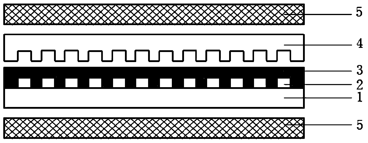
[0048] This embodiment provides a method for preparing a full-color micro-display device, comprising the following steps:
[0049] (1) Prepare an array of blue light Micro LED microchips 2 on the substrate 1 , the size of the blue light Micro LED microchips is preferably 50 μm, and the emission wavelength is preferably 450 nm.
[0050] (2) Prepare the resin glue containing the first embossed fluorescent material and the second embossed fluorescent material, wherein the first embossed fluorescent material is preferably II-VI group CdSe series quantum dot material, and its emission wavelength is preferably 628nm, half peak The width is preferably 35nm; the second embossed fluorescent material is preferably II-VI CdSe series quantum dot material, its emission wavelength is preferably 525nm, and its half-peak width is preferably 30nm. The main component of the resin glue is one or more of acrylic resins, polyurethanes, and epoxy resins, preferably acrylic thermosetting resins. Sp...
Embodiment 2
[0058] This embodiment provides a method for preparing a full-color micro-display device, which is basically similar to that of Embodiment 1, the main difference being that the curing method is changed from thermal curing to light curing. Compared with the thermal curing method, the light curing method does not need to heat the entire process, which avoids the thermal deformation of the substrate, microchip and template at high temperature, so the accuracy is higher; at the same time, there is no need to transfer the imprinted device to the temperature providing device , the curing time is shorter, and the curing process is also simplified; at the same time, the first or second imprint template can also be treated without infiltration, and the infiltration energy of the treated template and red and green quantum dot resin glue is reduced, which can be more conveniently processed. Mold removal and cleaning treatment reduce the difficulty of the process.
[0059] Specifically, t...
PUM
 Abstract
Description
Claims
Application Information


