
Eureka
For R&D, Eureka makes reading and utilizing patents & technical documents easy.
Eureka AIR
Designed for self-driven R&D workflows. Generate viable solutions, solve complex R&D challenges, empower your innovation with AI.

Eureka Materials
Designed for material experts only. Revolutionize your material R&D, from search, analyze, to developing new materials.

TechResearch
Generate reliable direction feasibility study reports for your R&D in just a few steps.

TechSeek
Discover and master advanced knowledge NOW. Basics, ideas, possibilities, all at once.

TechMind
As an expert in R&D Theories, TechMind can generates customized viable solutions instantly.

TechRisk
Analyze your overall solution with one click, know your potential R&D risks in advance.

TechMonitor
Get weekly tech updates, stay abreast of the latest tech innovations and key insights.
Wireless power supply wiring circuit board and battery module
- Summary
- Abstract
- Description
- Claims
- Application Information
AI Technical Summary
Benefits of technology
Problems solved by technology
Method used
Image

Examples
first embodiment
[0077](Wireless Power Supply Wiring Circuit Board of First Embodiment)
[0078]The following will describe First Embodiment of the present invention with reference to drawings.
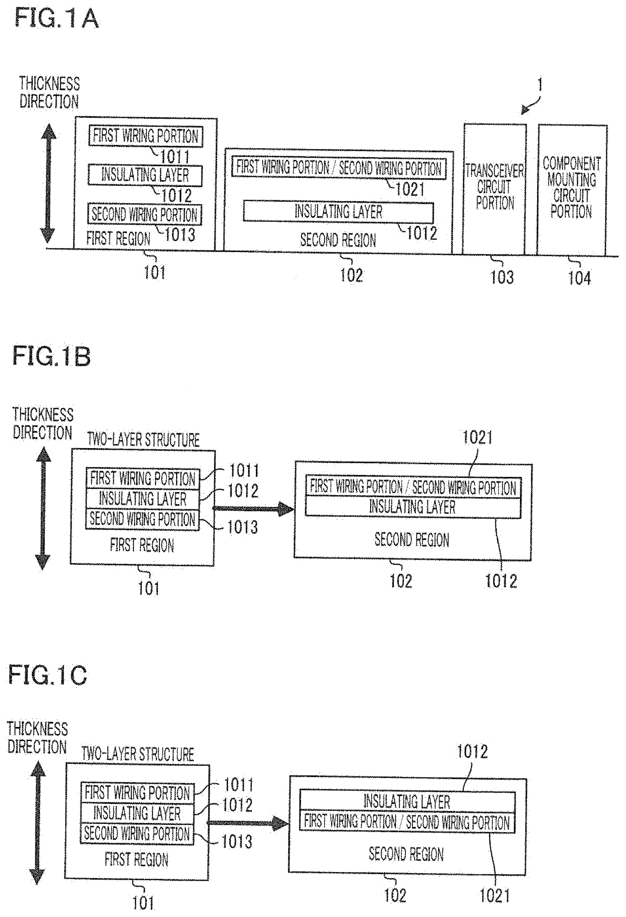
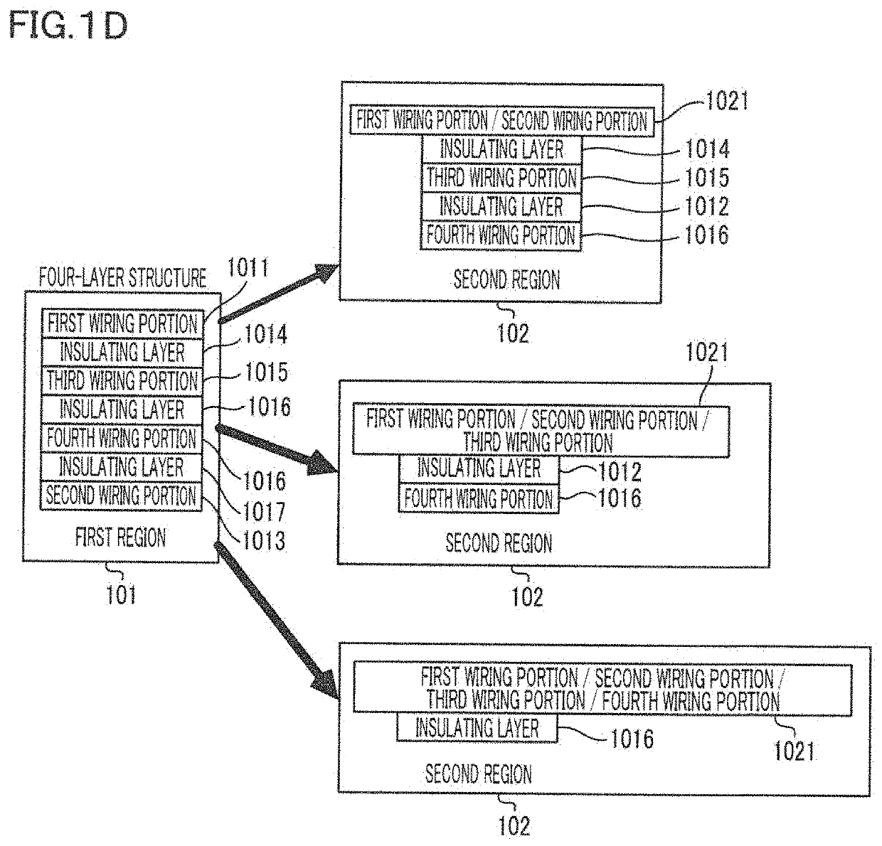
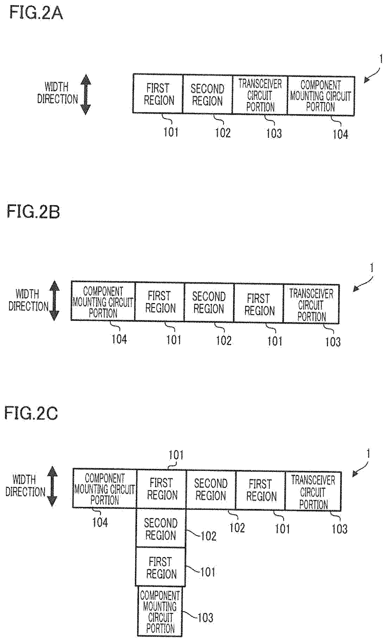
[0079]As shown in FIG. 1A, a wireless power supply wiring circuit board 1 includes an insulating layer 1012, a first wiring portion 1011 which is provided on one surface side in the thickness direction of the insulating layer 1012, a first region 101 including a second wiring portion 1013 which is provided on the other side in the thickness direction of the insulating layer 1012, a second region 102 in which the first wiring portion 1011 and the second wiring portion 1013 are provided on the same flat plane, a transceiver circuit portion 103, and a component mounting circuit portion 104 which is electrically connected to the transceiver circuit portion 103.
[0080]In this regard, as shown in FIG. 1B and FIG. 1C, the expression “provided on one surface side in the thickness direction” in the first region 101 may ind...
second embodiment
[0093](Wireless Power Supply Wiring Circuit Board of Second Embodiment)
[0094]The following will describe Second Embodiment of the present invention with reference to drawings. Members identical with those of First Embodiment will be denoted by the same reference numerals.
[0095]As shown in FIG. 6A and FIG. 6B, the wireless power supply wiring circuit board 1 includes a coil portion 11 configured to convert an electromagnetic wave to AC power, a first wiring portion 12 which is connected to the coil portion 11 and in which two conductive layers 122 and 124 receiving the AC power are stacked, and a first bending portion 13 which is provided to traverse the first wiring portion 12 and causes the inner side of the bend of the first wiring portion 12 to be recessed. The first bending portion 13 includes a first bending conductive layer 131 in which a conductive layer 124 formed on the inner side of the bend of the first wiring portion 12 is integrated with a conductive layer 122 formed on...
PUM
| Property | Measurement | Unit |
|---|---|---|
| Thickness | aaaaa | aaaaa |
| Thickness | aaaaa | aaaaa |
| Thickness | aaaaa | aaaaa |
Abstract
Description
Claims
Application Information
 - R&D Engineer
- R&D Manager
- IP Professional
- Industry Leading Data Capabilities
- Powerful AI technology
- Patent DNA Extraction
Browse by: Latest US Patents, China's latest patents, Technical Efficacy Thesaurus, Application Domain, Technology Topic, Popular Technical Reports.
© 2024 PatSnap. All rights reserved.Legal|Privacy policy|Modern Slavery Act Transparency Statement|Sitemap|About US| Contact US: help@patsnap.com