High-density capacitive device and method for manufacturing such a device
- Summary
- Abstract
- Description
- Claims
- Application Information
AI Technical Summary
Benefits of technology
Problems solved by technology
Method used
Image

Examples
Embodiment Construction
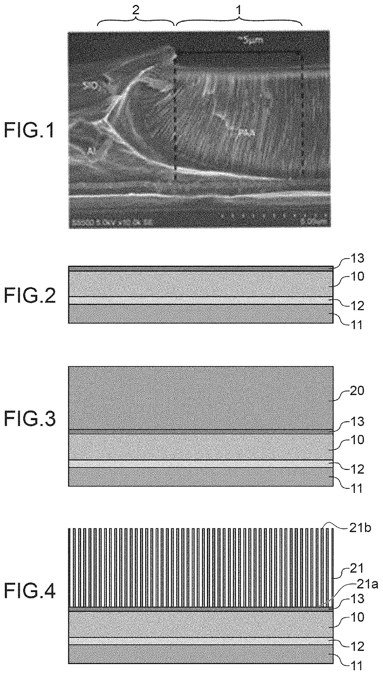
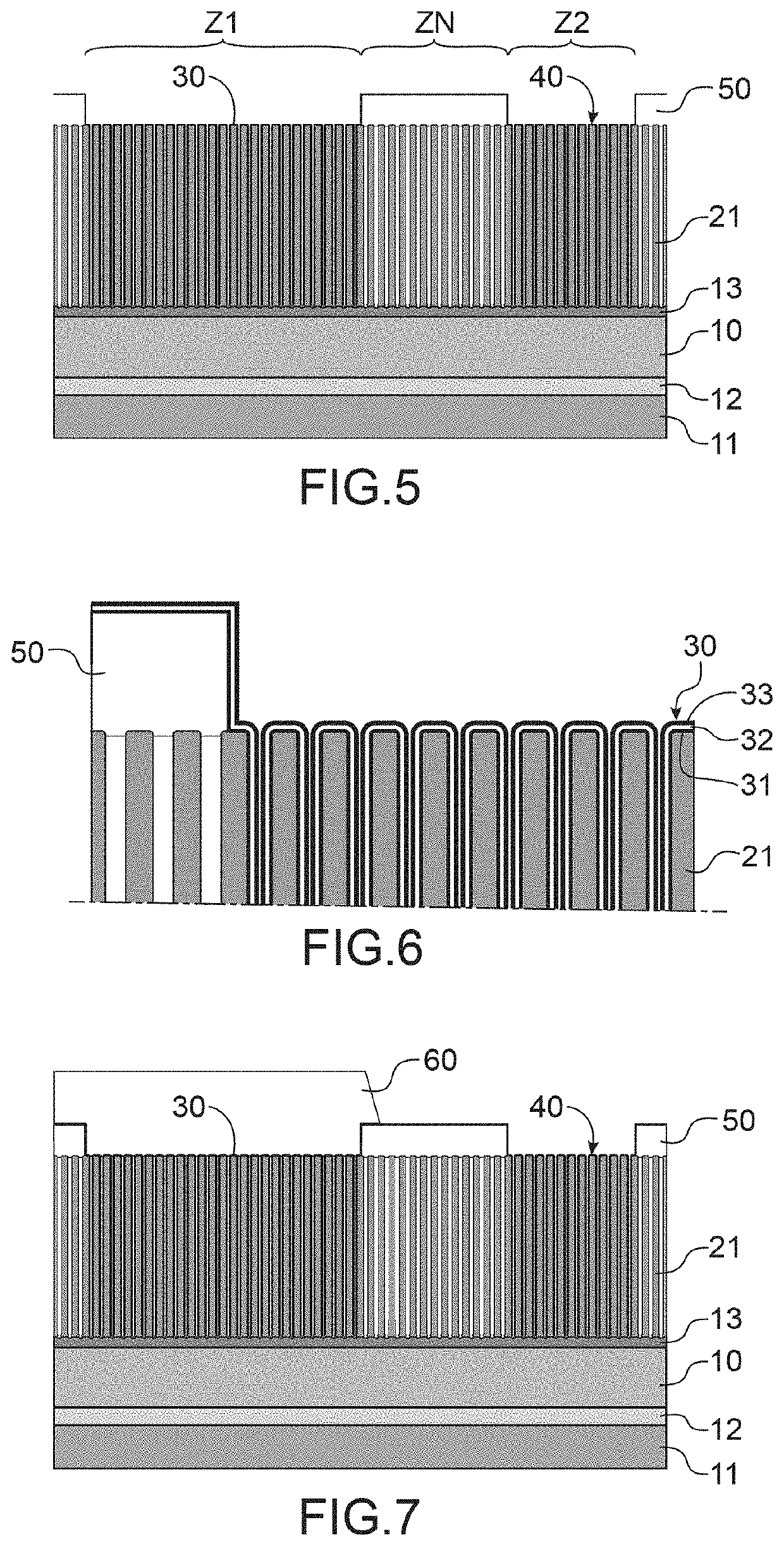
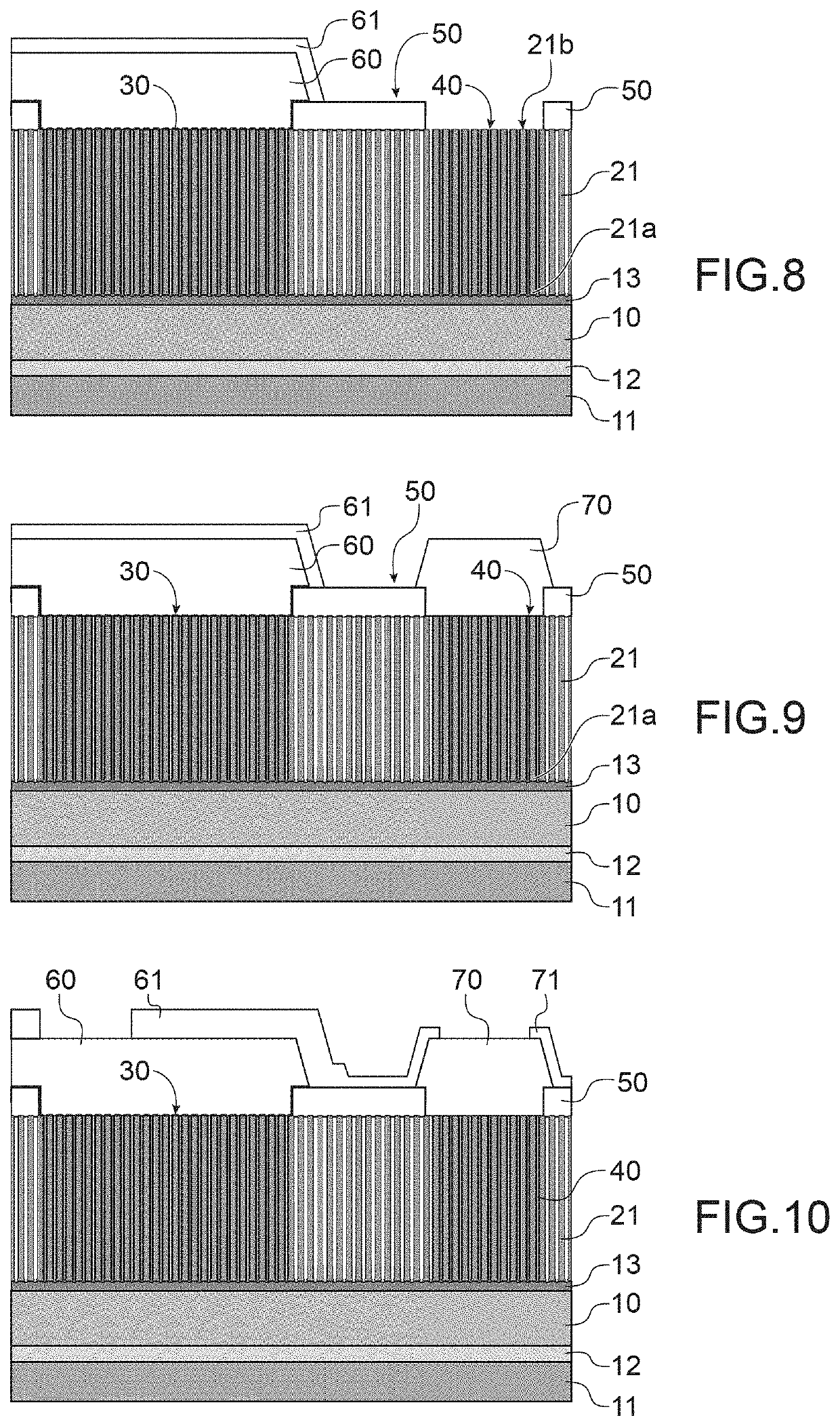
[0103]Although this is not limiting in any manner whatsoever, the invention finds particular applications in the field of high-density capacitances of more than 1 μF / mm2. Advantageously, the capacitive device may be integrated into a structure comprising other components.
[0104]We will now describe in more details a method for manufacturing a capacitive device according to a particular embodiment of the invention with reference to FIGS. 2 to 11.
[0105]The principle of the method of the invention consists in generating “full-sheet” (also called full-plate”) porous alumina layers.
[0106]The method comprises the following steps:
[0107]manufacturing of a base substrate (“base wafer”) through the following steps a), b) and c):
[0108]providing a metallic layer 10 (FIG. 2),
[0109]b) depositing a full-sheet aluminium layer 20 (FIG. 3),
[0110]c) structuring pores in the aluminium layer 20 by a full-sheet anodic etching process, subsequently to which a continuous porous alumina layer 21 is obtained ...
PUM
 Abstract
Description
Claims
Application Information
 - R&D Engineer
- R&D Manager
- IP Professional
- Industry Leading Data Capabilities
- Powerful AI technology
- Patent DNA Extraction
Browse by: Latest US Patents, China's latest patents, Technical Efficacy Thesaurus, Application Domain, Technology Topic.
© 2024 PatSnap. All rights reserved.Legal|Privacy policy|Modern Slavery Act Transparency Statement|Sitemap