
Semiconductor device

a technology of semiconductor devices and semiconductor chips, applied in semiconductor devices, semiconductor/solid-state device details, electrical apparatus, etc., can solve the problems of difficult thermal design and affecting the thermal interference between the two types of chips, and achieve the effect of suppressing thermal interference between the mosfet chip and the sbd chip and facilitating thermal design

Pending Publication Date: 2022-09-22
MITSUBISHI ELECTRIC CORP
View PDF0 Cites 0 Cited by
  • Summary
  • Abstract
  • Description
  • Claims
  • Application Information

AI Technical Summary

Benefits of technology

The semiconductor device described in this patent reduces thermal interference between two types of chips, which makes it easier to design the heat management system. This means that the chips can generate heat without affecting each other, making the overall performance better.

Problems solved by technology

In the semiconductor device of Japanese Patent Application Laid-Open No. 2005-310907, the MOSFET chips and the SBD chips are mounted on the same die pad, greatly affecting the thermal interference between the both types of chips.
Therefore, a difference in the values of thermal resistancesed between the case where the thermal resistances are measured under the actual use where the both types of chips generate heat under various conditions and the case where the thermal resistances are measured for individual types of chips, and this has been the problem that has made thermal design difficult.

Method used


Image

  • Semiconductor device
  • Semiconductor device
  • Semiconductor device

Examples


embodiment 1

A. Embodiment 1

[0025]

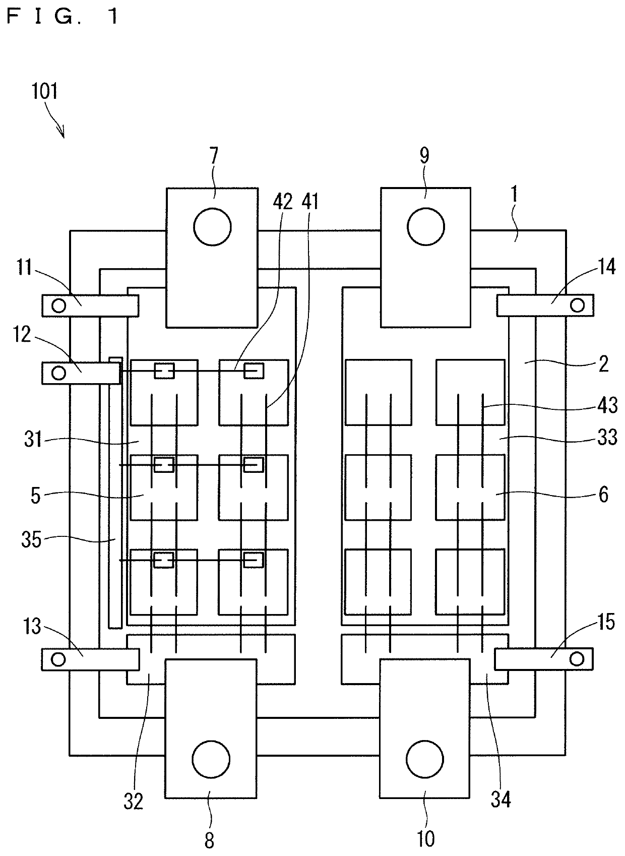
[0026]FIG. 1 is a plan view of a semiconductor device 101 of Embodiment 1. The semiconductor device 101 includes a base plate 1, an insulating substrate 2, patterns 31, 32, 33, 34, and 35 being conductive patterns, a plurality of MOSFET chips 5, a plurality of SBD chips 6, a drain main terminal 7, a source main terminal 8, a cathode main terminal 9, an anode main terminal 10, a drain auxiliary terminal 11, a gate auxiliary terminal 12, a source auxiliary terminal 13, a cathode auxiliary terminal 14, and an anode auxiliary terminal 15.

[0027]The insulating substrate 2 is mounted on the base plate 1. The patterns 31, 32, 33, 34, and 35 are formed on the insulating substrate 2.

[0028]The plurality of MOSFET chips 5 are mounted on the pattern 31. Each MOSFET chip 5 has a drain electrode on the lower surface thereof and a source electrode and a gate electrode on the upper surface thereof. Therefore, by mounting each MOSFET chip 5 on the pattern 31, the drain electrode ...

embodiment 2

B. Embodiment 2

[0045]

[0046]FIG. 7 is a plan view of a semiconductor device 201 of Embodiment 2. In the semiconductor device 101 of Embodiment 1, the patterns 31 and 32 on which the plurality of MOSFET chips 5 are mounted and the patterns 33 and 34 on which the plurality of SBD chips 6 are mounted are provided on the same insulating substrate 2. Whereas, in the semiconductor device 201 of Embodiment 2, the patterns 31 and 32 on which the plurality of MOSFET chips 5 are mounted and the patterns 33 and 34 on which the plurality of SBD chips 6 are mounted are provided on different insulating substrates 21 and 22, respectively. That is, the insulating substrates 21 and 22 are mounted on the base plate 1 in the semiconductor device 201. And, the patterns 31 and 32 are formed on the insulating substrate 21, and the patterns 33 and 34 are formed on the insulating substrate 22. The configuration of semiconductor device 201 other than the above is the same as the semiconductor device 101.

[004...

embodiment 3

C. Embodiment 3

[0054]

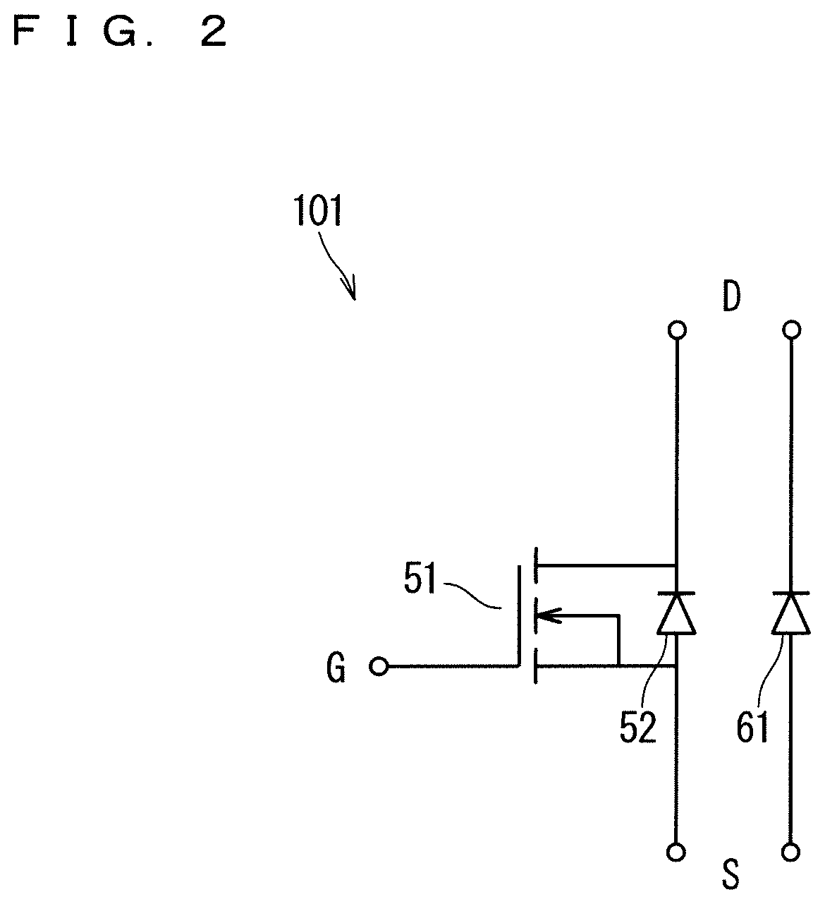
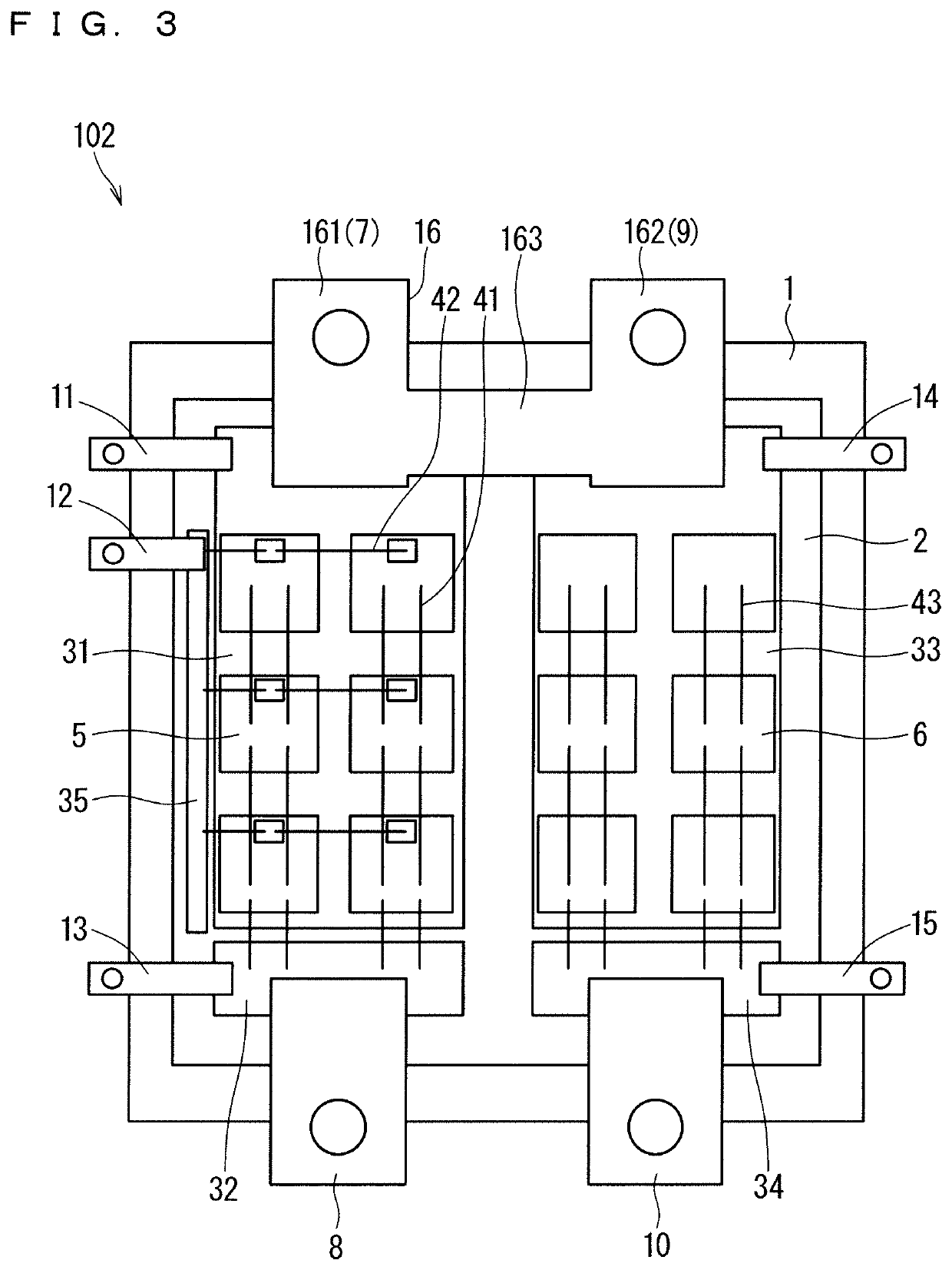
[0055]FIG. 10 is a plan view of a semiconductor device 301 of Embodiment 3. In Modification 1 of Embodiment 1, the drain main terminal 7 and the cathode main terminal 9 are connected by being configured by the common terminal 16. Instead of this, in the semiconductor device 301, the pattern 31 being the drain conductive pattern and the pattern 33 being the cathode conductive pattern 33 are connected by conductive wires 44, so that the drain main terminal 7 and the cathode main terminal 9 are electrically connected. The configuration of semiconductor device 301 other than the above is the same as the semiconductor device 101 of Embodiment 1. An equivalent circuit diagram of the semiconductor device 301 is the same as the equivalent circuit diagram of the semiconductor device 102 illustrated in FIG. 4.

[0056]

[0057]In the semiconductor device 301 of Embodiment 3, the pattern 31 being the drain conductive pattern and the pattern 33 being the cathode conductive patter...


PUM

PropertyMeasurementUnit
conductiveaaaaaaaaaa
currentaaaaaaaaaa
wiring inductanceaaaaaaaaaa

Abstract

An object of the present disclosure is to facilitate thermal design in a semiconductor device in which MOSFETs and SBDs are connected in antiparallel. The semiconductor device includes a MOSFET chip provided on a first pattern, whose drain electrode and source electrode are electrically connected to the first pattern and a second pattern, respectively, an SBD chip provided on a third pattern, whose cathode electrode and anode electrode are electrically connected to the third pattern and fourth pattern, respectively, a drain main terminal connected to the first pattern, a source main terminal connected to the second pattern, a cathode main terminal connected to the third pattern, and an anode main terminal connected to the fourth pattern. At least one of between the drain main terminal and the cathode main terminal and between the source main terminal and the anode main terminal is not electrically connected.

Description

BACKGROUND OF THE INVENTIONField of the Invention[0001]The present disclosure relates to a semiconductor device.Description of the Background Art[0002]Japanese Patent Application Laid-Open No. 2005-310907 discloses semiconductor device including Metal-Oxide-Semiconductor Field Effect Transistors (MOSFET) and Schottky Barrier Diodes (SBD) connected in antiparallel to the MOSFETs, in which the GNDs are used for the MOSFETs and the SBDs in a separate manner. According to the configuration of the semiconductor device, the forward voltage Vf can be measured individually for the MOSFETs and the SBDs, and the thermal resistances of the MOSFETs and the SBDs can be measured individually from the temperature dependence of the respective forward voltage Vf.SUMMARY[0003]In the semiconductor device of Japanese Patent Application Laid-Open No. 2005-310907, the MOSFET chips and the SBD chips are mounted on the same die pad, greatly affecting the thermal interference between the both types of chips...

Claims


Application Information

Patent Timeline
Patent Type & Authority Applications(United States)
IPC IPC(8): H01L25/07H01L25/18H01L23/00H01L23/492
CPCH01L25/072H01L25/18H01L24/48H01L23/492H01L2224/48137H01L2224/48175H01L2924/12032H01L2924/13091H01L2924/30107H01L23/49838H01L23/50H01L2224/4917H01L2224/0603H01L2224/49113H01L24/49H01L2924/19107H01L2224/49175H01L2924/00014H01L24/06H01L2224/04042H01L23/5386H01L2224/45099
Inventor MIKAMI, KAZUTO
Owner MITSUBISHI ELECTRIC CORP
Learn More