Supercharge Your Innovation With Domain-Expert AI Agents!

Electronic component module

Pending Publication Date: 2022-09-29
MURATA MFG CO LTD
View PDF0 Cites 0 Cited by
  • Summary
  • Abstract
  • Description
  • Claims
  • Application Information

AI Technical Summary

Benefits of technology

The present disclosure provides a double-sided mount electronic component module that can be obtained in a simple process and have high isolation between components. The module has a first conductive member mounted on the substrate, which simultaneously mounts the first electronic component and the second electronic component, achieving high isolation between them. The first shield film is connected to the first conductive member, further improving the isolation. This simple process achieves a double-sided mount electronic component module with high isolation between components.

Problems solved by technology

However, in the conventional high frequency module, a process of forming a shield wall by laser machining or the like, the multilayer wiring substrate may be damaged.

Method used


Image

  • Electronic component module
  • Electronic component module
  • Electronic component module

Examples


first exemplary embodiment

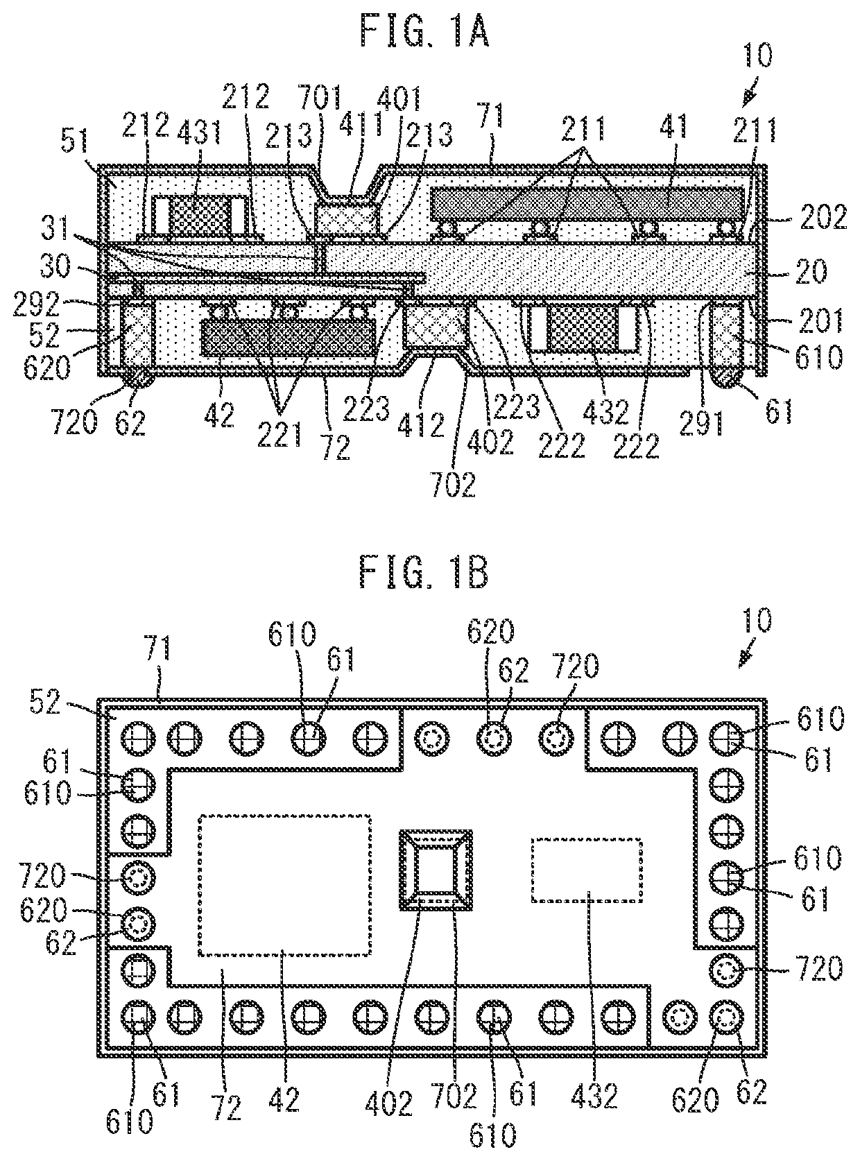
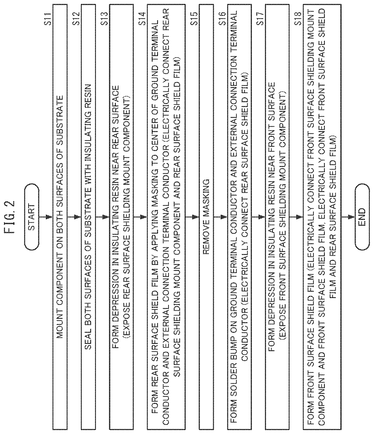
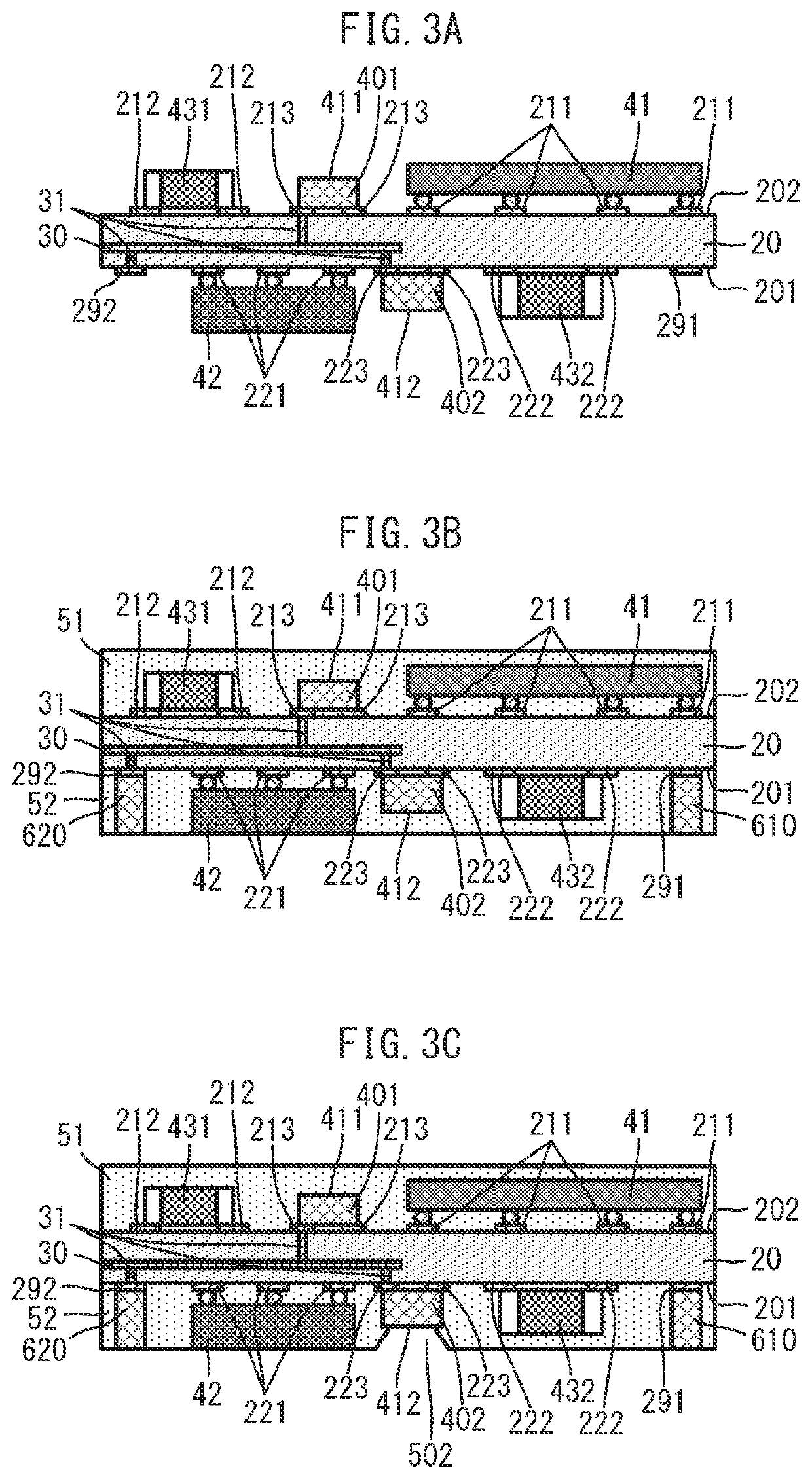
[0019]An electronic component module according to a first exemplary embodiment of the present disclosure will be described with reference to drawings. FIG. 1A is a side cross-sectional view showing a configuration of the electronic component module according to the first exemplary embodiment of the present disclosure, and FIG. 1B is a rear view of the electronic component module according to the first exemplary embodiment. It is to be noted that, in FIG. 1B, in order to easily distinguish between an external connection terminal conductor and a ground terminal conductor, hatching is added to a solder bump of the external connection terminal conductor.

[0020]As shown in FIG. 1A and FIG. 1B, an electronic component module 10 includes a substrate 20, a mount electronic component 41, a mount electronic component 42, a mount electronic component 431, a mount electronic component 432, a second conductive member 401, a first conductive member 402, an insulating resin 51, an insulating resin ...

second exemplary embodiment

[0067]An electronic component module according to a second exemplary embodiment of the present disclosure will be described with reference to the drawings. FIG. 5A is a side cross-sectional view showing a configuration of the electronic component module according to the second exemplary embodiment of the present disclosure, and FIG. 5B is a rear view of the electronic component module according to the second exemplary embodiment. It is to be noted that, in FIG. 5B, in order to easily distinguish between an external connection terminal conductor and a ground terminal conductor, hatching is added to a solder bump of the external connection terminal conductor.

[0068]As shown in FIG. 5A and FIG. 5B, the electronic component module 10A according to the second exemplary embodiment is different in disposition of the shield film 72 from the electronic component module 10 according to the first exemplary embodiment. Other configurations of the electronic component module 10A are the same as o...

third exemplary embodiment

[0071]An electronic component module according to a third exemplary embodiment of the present disclosure will be described with reference to the drawings. FIG. 6A is a side cross-sectional view showing a configuration of the electronic component module according to the third exemplary embodiment of the present disclosure, and FIG. 6B is a rear view of the electronic component module according to the third exemplary embodiment. It is to be noted that, in FIG. 6B, in order to easily distinguish between an external connection terminal conductor and a ground terminal conductor, hatching is added to a solder bump of the external connection terminal conductor.

[0072]As shown in FIG. 6A and FIG. 6B, an electronic component module 10B according to the third exemplary embodiment is different from the electronic component module 10 according to the first exemplary embodiment in that the shield film 72 and the shield film 71 are not connected on the outer surface of the insulating resin 52. Oth...


PUM


Abstract

An electronic component module includes a substrate with a first main surface and a second main surface. Mount electronic components and a second conductive member are mounted on the second main surface, and the second conductive member is disposed between the mount electronic component and the mount electronic component. The second conductive member is connected to a shield film disposed near the second main surface through a depression. Mount electronic components and a first conductive member are mounted on the first main surface, and the first conductive member is disposed between the mount electronic component and the mount electronic component. The first conductive member is connected to a shield film disposed near the first main surface through a depression.

Description

CROSS REFERENCE TO RELATED APPLICATION[0001]This is a continuation of International Application No. PCT / JP2020 / 043595 filed on Nov. 24, 2020 which claims priority from Japanese Patent Application No. 2019-229952 filed on Dec. 20, 2019. The contents of these applications are incorporated herein by reference in their entireties.BACKGROUND OF THE DISCLOSUREField of the Disclosure[0002]The present disclosure relates to an electronic component module in which a plurality of electronic components are mounted on a substrate.Description of the Related Art[0003]Patent Literature 1 discloses a high frequency module in which a plurality of components are mounted on a bottom surface of a multilayer wiring substrate. A shield wall is disposed between the components on the bottom surface of the multilayer wiring substrate.[0004]The shield wall is provided by forming a groove in a sealing resin layer formed on the bottom surface of the multilayer wiring substrate, and then filling the groove with ...

Claims


Application Information

Patent Timeline
IPC IPC(8): H01F27/29H05K3/46H01F27/28
CPCH01F27/292H05K3/4685H01F27/2804H05K9/00H01L23/12H05K1/0216H05K1/181H05K3/284H01L23/3121H01L21/56H01L23/552H01L24/17H01L25/165
Inventor KOMIYAMA, MINORUKUSUNOKI, MOTOHIKOISHIDO, MITSUOKOMATSU, TORU
Owner MURATA MFG CO LTD
Features
  • R&D
  • Intellectual Property
  • Life Sciences
  • Materials
  • Tech Scout
  • Unparalleled Data Quality
  • Higher Quality Content
  • 60% Fewer Hallucinations
Learn More