Eureka AIR delivers breakthrough ideas for toughest innovation challenges, trusted by R&D personnel around the world.

Semantic image segmentation for semiconductor-based applications

Pending Publication Date: 2022-10-06
KLA TENCOR CORP
View PDF0 Cites 0 Cited by
  • Summary
  • Abstract
  • Description
  • Claims
  • Application Information

AI Technical Summary

Benefits of technology

The patent describes a system and method for determining information about a specimen by assigning labels to multiple pixels in an image and using those labels to determine the information without needing a reference image. The system and method use a semantic segmentation model to assign labels to the image, which can be useful for identifying different parts of the specimen. This technology can be used in a variety of applications, such as medical diagnostics or materials science.

Problems solved by technology

However, as the dimensions of semiconductor devices decrease, inspection becomes even more important to the successful manufacture of acceptable semiconductor devices because smaller defects can cause the devices to fail.
There are several disadvantages to using a reference image in the applications described above.
In addition, many currently used defect inspection algorithms are based on detecting defects in a difference image, but in some cases it can be difficult or even impossible to generate a difference image when there is no suitable reference.
Techniques like standard reference die (SRD) have been developed for such situations, but the success of such techniques often rests on the assumption that the original die is free of defects, which is not necessarily the case.
Similar difficulties can also arise in relative metrology measurements and defect review re-detection.

Method used


Image

  • Semantic image segmentation for semiconductor-based applications
  • Semantic image segmentation for semiconductor-based applications
  • Semantic image segmentation for semiconductor-based applications

Examples


Embodiment Construction

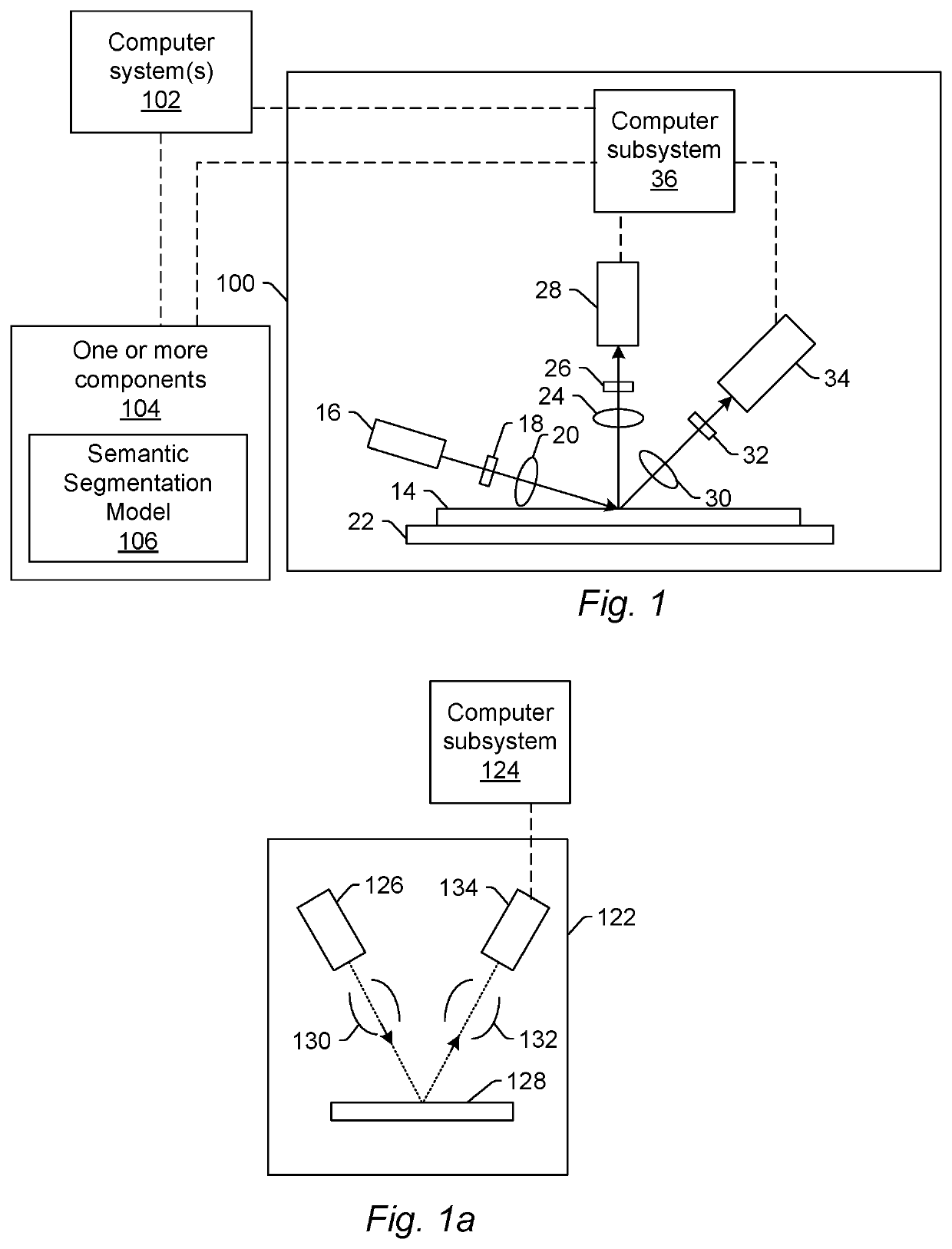
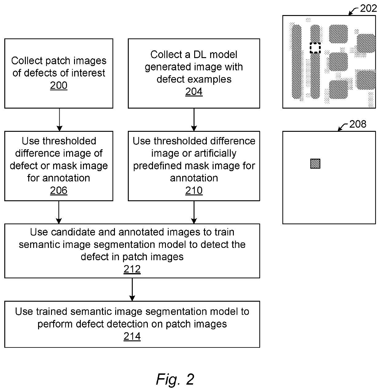
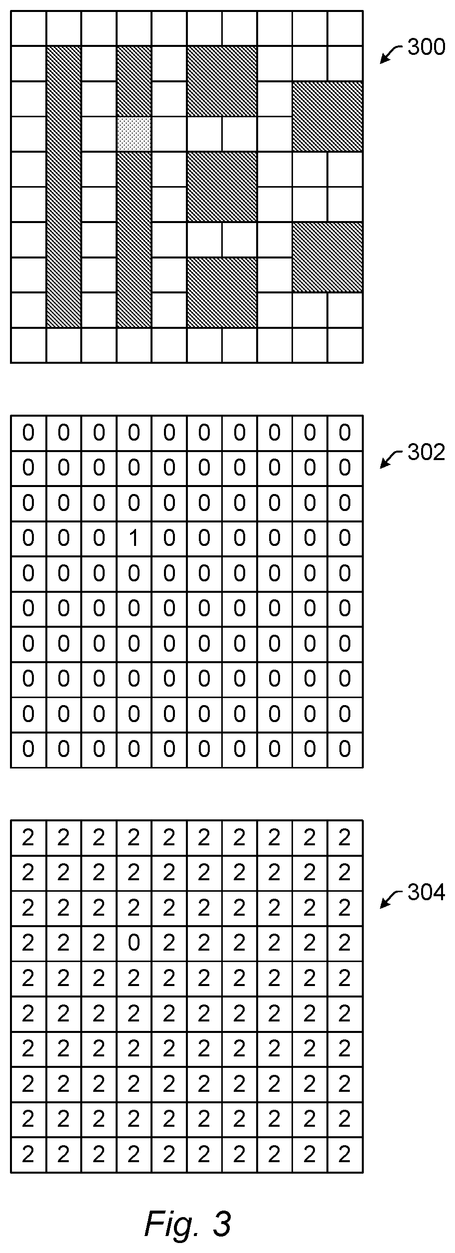
[0023]The terms “design,”“design data,” and “design information” as used interchangeably herein generally refer to the physical design (layout) of an IC or other semiconductor device and data derived from the physical design through complex simulation or simple geometric and Boolean operations. The design may include any other design data or design data proxies described in commonly owned U.S. Pat. No. 7,570,796 issued on Aug. 4, 2009 to Zafar et al. and U.S. Pat. No. 7,676,077 issued on Mar. 9, 2010 to Kulkarni et al., both of which are incorporated by reference as if fully set forth herein. In addition, the design data can be standard cell library data, integrated layout data, design data for one or more layers, derivatives of the design data, and full or partial chip design data. Furthermore, the “design,”“design data,” and “design information” described herein refers to information and data that is generated by semiconductor device designers in a design process and is therefore ...


PUM


Abstract

Methods and systems for determining information for a specimen are provided. One system includes a computer subsystem and one or more components executed by the computer subsystem. The one or more components include a semantic segmentation model configured for assigning labels to each of multiple pixels in an image responsive to what is represented in each of the multiple pixels. The image is an image of a specimen generated by an imaging subsystem. The computer subsystem is configured for determining information for the specimen from the assigned labels and without a reference image for the specimen.

Description

BACKGROUND OF THE INVENTION1. Field of the Invention[0001]The present invention generally relates to methods and systems for determining information for a specimen. Certain embodiments relate to a semantic segmentation model configured for assigning labels to each of multiple pixels in a specimen image.2. Description of the Related Art[0002]The following description and examples are not admitted to be prior art by virtue of their inclusion in this section.[0003]Fabricating semiconductor devices such as logic and memory devices typically includes processing a substrate such as a semiconductor wafer using a large number of semiconductor fabrication processes to form various features and multiple levels of the semiconductor devices. For example, lithography is a semiconductor fabrication process that involves transferring a pattern from a reticle to a resist arranged on a semiconductor wafer. Additional examples of semiconductor fabrication processes include, but are not limited to, ch...

Claims


Application Information

Patent Timeline
IPC IPC(8): G06T7/00G06T7/10G06V20/70G06V10/774G06N3/08
CPCG06T7/0004G06T7/10G06V20/70G06V10/7747G06N3/08G06T2207/30148G06T2207/20081G06T2207/10061G06T2207/20084G06V10/26G06V10/774G06V10/82G06V2201/06G06N3/094G06N3/0475G06N3/0455G06N3/0464G06T2207/10081
Inventor BRAUER, BJORNWALLINGFORD, RICHARD
Owner KLA TENCOR CORP
Why Eureka
Eureka Blog
Learn More