Method and structure for thin-film fabrication

a thin-film fabrication and structure technology, applied in the direction of basic electric elements, electrical equipment, semiconductor devices, etc., can solve the problems of limiting the release film size, and affecting the effect of production efficiency

a thin-film fabrication and structure technology, applied in the direction of basic electric elements, electrical equipment, semiconductor devices, etc., can solve the problems of limiting the release film size, and affecting the effect of production efficiency

US20220367275A1Pending Publication Date: 2022-11-17OKSANEN JANI +1

Image

  • Method and structure for thin-film fabrication
  • Method and structure for thin-film fabrication
  • Method and structure for thin-film fabrication

Examples


Embodiment Construction

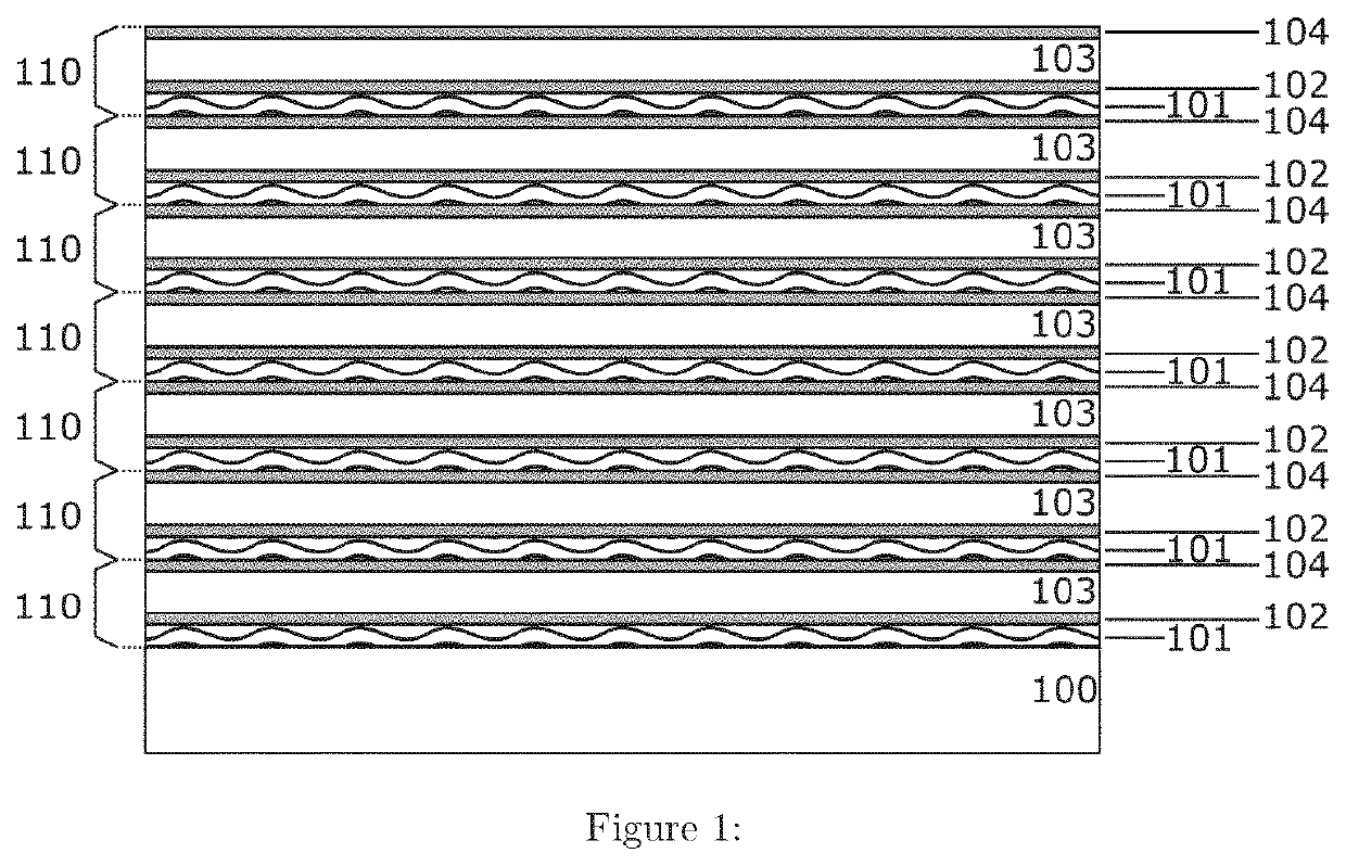
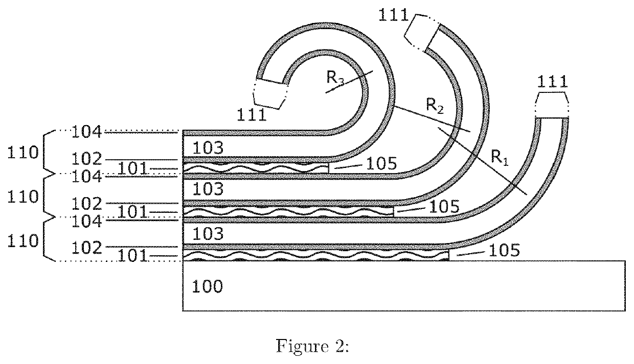
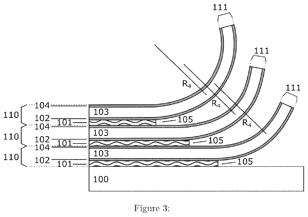
[0022]In the following detailed description of the invention and the drawings, III-V materials or III-V semiconductors refer to materials that consist of at least one element from the group III (or 13) of the periodic table (such as aluminum (Al), gallium (Ga) or indium (In)) and at least one element of the group V (or 15) of the periodic table (such as nitrogen (N), phosphorus (P), arsenic (As) or antimony (Sb). Thin films or thin semiconductor films refer to films of III-V semiconductors or other semiconductors or materials that are generally 0.1 nm-1000 μm, or preferably 10 nm-10 μm thick. Typically (but not necessarily), device or component layers are 1 nm-100 μm, or preferably 10 nm-10 μm, thick, while each strained layer may be even 1 monolayer, or up to several hundreds of nanometers thick. Regarding the descriptions of the positions of the layers, directly below a layer refers to a position next to the said layer on the side of the parent substrate, and directly above a laye...


PUM


Abstract

The present invention relates to the epitaxial lift-off of thin-films allowing the reuse of the expensive semiconductor substrates. In particular, it describes a structure and a method for epitaxial lift-off of several thin films from a single substrate (100) using a plurality of dissimilar sacrificial layers (101), strained layers (102, 104), and / or device or component layers (103). The properties of the sacrificial layers (101) and the strained layers (102,104) can be used (i) to facilitate the lift off process, (ii) to control the point of time of release of each released thin film individually and (iii) to aid in separation and sorting of the released thin films. The released device or component layers can comprise various useful structures, such as optoelectronic devices photonic components.

Description

INTRODUCTION[0001]III-V materials are often though of as the workhorse of the optoelectronics industry due to their typically direct band gaps, high carrier mobilities and band gap values suitable for e.g. optical communications and high-performance solar cells. However, their inherent drawback is the relatively high cost of the substrates. To circumvent this, various approaches have been explored to create thin-film devices that are released from the growth substrate, allowing substrate re-use and incurring significant cost reductions. In terms of cost-effectiveness epitaxial lift-off (ELO) has been identified as the most promising approach [1]. In addition to the cost savings via substrate re-use, the thin-film devices have the advantages of flexibility and the possibility of integration to various everyday materials.[0002]In epitaxial lift-off, a sacrificial layer is grown on a parent substrate, followed by various layers that typically constitute a device structure, such as a so...

Claims


Application Information

Patent Timeline
17 Nov 2022
Publication
US20220367275A1
IPC
H01L21/78; H01L31/18
CPC
H01L21/7813; H01L31/1896; H01L31/0735; H01L31/184; Y02E10/544
Inventors
OKSANEN, JANI; HAGGRÉN, TUOMAS